SLUSDC1 September 2018 UCD90320U
PRODUCTION DATA.
- 1 Features
- 2 Applications
- 3 Description
- 4 Revision History
- 5 Description Continued
- 6 Pin Configuration and Functions
- 7 Specifications
-
8 Detailed Description
- 8.1 Overview
- 8.2 Functional Block Diagram
- 8.3 Feature Description
- 8.4
Device Functional Modes
- 8.4.1 Rail Monitoring Configuration
- 8.4.2 GPI Configuration
- 8.4.3 Rail Sequence Configuration
- 8.4.4 Fault Responses Configuration
- 8.4.5 GPO Configuration
- 8.4.6 Margining Configuration
- 8.4.7 Pin Selected Rail States Configuration
- 8.4.8 Watchdog Timer
- 8.4.9 System Reset Function
- 8.4.10 Cascading Multiple Devices
- 8.4.11 Rail Monitoring
- 8.4.12 Status Monitoring
- 8.4.13 Data and Error Logging to EEPROM Memory
- 8.4.14 Black Box First Fault Logging
- 8.4.15 PMBus Address Selection
- 8.4.16 ADC Reference
- 8.4.17 Device Reset
- 8.4.18 Brownout
- 8.4.19 Internal Fault Management
- 8.4.20 Single Event Upset
- 8.5 Device Configuration and Programming
- 9 Application and Implementation
- 10Power Supply Recommendations
- 11Layout
- 12Device and Documentation Support
- 13Mechanical, Packaging, and Orderable Information
Package Options
Mechanical Data (Package|Pins)
- ZWS|169
Thermal pad, mechanical data (Package|Pins)
Orderable Information
8.4.2 GPI Configuration
Up to 32 of the 84 GPIO pins of the UCD90320U device can be configured as GPI. The GPI configuration window is under the Pin Assignment tab. Figure 11 shows an example.
 Figure 11. GPI Configuration Window (Hard Configuration ► Monitors and GPIO Pins Assignment)
 The polarity of GPI pins can be configured to be either active high or active low. Each GPI can be used as a source of sequence dependency. (See also the Rail Sequence Configuration section). The GPI pins can be also used for cascading function. (See also the Cascading Multiple Devices section). The first defined 3 GPIs regardless of their main purpose are assigned to the pin selected states function. (See also the Pin Selected Rail States Configuration section).
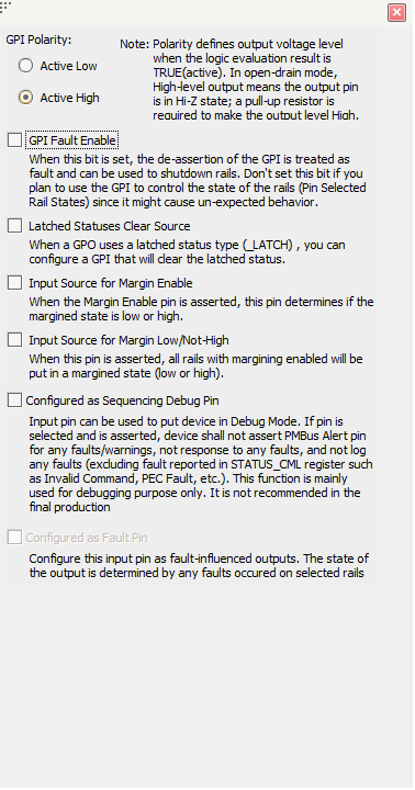
In addition hard configuration functions, four special behaviors can be assigned to each GPI pin using the dropdown window shown in Figure 12:
- GPI Fault The de-assertion of this pin is treated as a fault, which can trigger shut-down actions for any voltage rails. (See also the Fault Responses Configuration section).
- Latched Statuses Clear Source This pin can be used to clear latched-type statuses (_LATCH). (See also the GPO Configuration section).
- Input Source for Margin Enable When this pin is asserted, all rails with margining enabled enter into a margined state (low or high). This special behavior can be assigned to only one GPI.
- Input Source for Margin Low and Not-High When this pin is asserted, all margined rails are set to Margin Low as long as the Margin Enable is asserted. When this pin is de-asserted the rails are set to Margin High as long as the Margin Enable is asserted. This special behavior can be assigned to only one GPI.
- Configured as Debug Pin When the pin is asserted, the device does not alert the PMBALERT pin, and neither responds to, nor logs any faults as defined in Table 2. The device ignores the rail sequence ON and OFF dependency conditions. As soon as the sequence ON and OFF timeout expires, the rails are sequenced ON or OFF accordingly regardless of the timeout action. If the sequence ON or OFF timeout value is set to 0, the rails are sequenced ON or OFF immediately. The fault pins do not pull the fault bus low. LGPOs affected by these events return to the original states.
- Configured as Fault Pin GPI fault enable functionality must be set to enable this feature. When set, if there is no fault on a fault bus. The FAULT pin is digital input pin and it monitors the fault bus. When one or more UCD90329 devices detect a rail fault, the corresponding FAULT pin is turned into active driven low state, pulling down the fault bus voltage and informing all other UCD90320U devices of the corresponding fault. This behavior allows a coordinated action to be taken across multiple devices. After the fault is cleared, the state of the FAULT pin reverts to that of an input pin.(See also the Cascading Multiple Devices section).
 Figure 12. GPI Configuration Dropdown Window
(Hardware Configuration ► Monitor and GPIO Pins Assignment)
Table 2. List of Events Affected by Debug Mode
| Events | Description |
|---|---|
| VOUT_OV_FAULT | Voltage rail is over OV fault threshold |
| VOUT_OV_WARNING | Voltage rail is over OV warning threshold |
| VOUT_UV_FAULT | Voltage rail is under UV fault threshold |
| VOUT_UV_WARNING | Voltage rail is under UV warning threshold |
| TON_MAX | Voltage rail fails to reach power good threshold in predefined period. |
| TOFF_MAX Warning | Voltage rail fails to reach power not good threshold in predefined period |
| IOUT_OC_FAULT | Current rail is over OC fault threshold |
| IOUT_OC_WARNING | Current rail is under OC warning threshold |
| IOUT_UC | Current rail is under UC fault threshold |
| OT_FAULT | Temperature rail is over OT fault threshold |
| OT_WARNING | Temperature rail is over OT warning threshold |
| All GPI de-asserted | No logging and fault response, but the function of the GPI is not ignored. |
| SYSTEM_WATCHDOG_TIMEOUT | System watch timeout |
| RESEQUENCE_ERROR | Rail fails to resequence |
| SEQ_ON_TIMEOUT | Rail fails to meeting sequence on dependency in predefined period |
| SEQ_OFF_TIMEOUT | Rail fails to meeting sequence on dependency in predefined period |
| SLAVE_FAULT | Rail is shut down due to that its master has fault |
| SINGLE_EVENT_UPSET | SEU is detected on the configuration SRAM |