SLUSDC1 September 2018 UCD90320U
PRODUCTION DATA.
- 1 Features
- 2 Applications
- 3 Description
- 4 Revision History
- 5 Description Continued
- 6 Pin Configuration and Functions
- 7 Specifications
-
8 Detailed Description
- 8.1 Overview
- 8.2 Functional Block Diagram
- 8.3 Feature Description
- 8.4
Device Functional Modes
- 8.4.1 Rail Monitoring Configuration
- 8.4.2 GPI Configuration
- 8.4.3 Rail Sequence Configuration
- 8.4.4 Fault Responses Configuration
- 8.4.5 GPO Configuration
- 8.4.6 Margining Configuration
- 8.4.7 Pin Selected Rail States Configuration
- 8.4.8 Watchdog Timer
- 8.4.9 System Reset Function
- 8.4.10 Cascading Multiple Devices
- 8.4.11 Rail Monitoring
- 8.4.12 Status Monitoring
- 8.4.13 Data and Error Logging to EEPROM Memory
- 8.4.14 Black Box First Fault Logging
- 8.4.15 PMBus Address Selection
- 8.4.16 ADC Reference
- 8.4.17 Device Reset
- 8.4.18 Brownout
- 8.4.19 Internal Fault Management
- 8.4.20 Single Event Upset
- 8.5 Device Configuration and Programming
- 9 Application and Implementation
- 10Power Supply Recommendations
- 11Layout
- 12Device and Documentation Support
- 13Mechanical, Packaging, and Orderable Information
Package Options
Mechanical Data (Package|Pins)
- ZWS|169
Thermal pad, mechanical data (Package|Pins)
Orderable Information
8.4.6 Margining Configuration
The UCD90320U device provides accurate closed-loop margining for up to 24 voltage rails. System reliability is improved through four-corner testing during system verification. During four-corner testing, the system operates at the minimum and maximum expected ambient temperature and with each power supply set to the minimum and maximum output voltage, commonly referred to as margining. Margining can be controlled via the PMBus interface using the OPERATION command or by configuring two GPI pins as margin-EN and margin-UP/DOWN inputs. The MARGIN_CONFIG command in the UCD90320U Sequencer and System Health Controller PMBus Command Reference user guide describes several margining options, including ignoring faults while margining and using closed-loop margining to trim the rail output voltage.
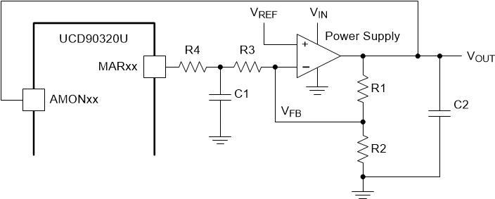
The device provides 24 PWM output pins for closed-loop margining. Figure 22 shows the block diagram of margining circuit. An external R-C network converts the PWM pulses into a DC margining voltage. The margining voltage is connected to the power supply feedback node through a resistor. The feedback node voltage is thus slightly pulled up or down by the margining voltage, causing the rail output voltage to change. The UCD90320U device monitors the rail output voltage. The device adjusts the margining PWM duty cycle accordingly such that the rail output voltage is regulated at the margin-high or margin-low voltages defined by the user. Effectively, margin control loop of the UCD90320U device overwrites the DC set point of the margined power supply. The margin control loop is extremely slow in order in order to not interfere with the power supply control loop.
 Figure 22. Block Diagram of Margining Circuit
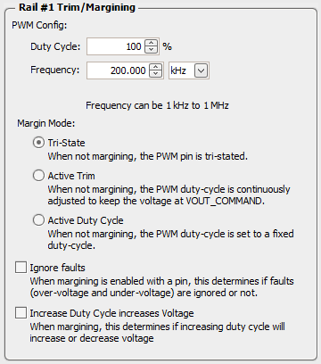
 Margining pins can be configured under the Pin Assignment tab, as shown in Figure 23. When not margining, the margin pin can operate in one of three modes:
- tri-state
- active trim
- active duty cycle
Tri-state mode sets the margin pin to high-impedance. Active Trim mode performs a continuously trim the DC output voltage. Active Duty Cycle mode provides a user-defined fixed PWM duty cycle as shown in Figure 23.
 Figure 23. Margining Configuration Dropdown Window (Hardware Configuration ► Monitor and GPIO Pin Assignment)