SLVSDD7B August 2016 – March 2022 UCD9090A
PRODUCTION DATA
- 1 Features
- 2 Applications
- 3 Description
- 4 Revision History
- 5 Pin Configuration and Functions
- 6 Specifications
-
7 Detailed Description
- 7.1 Overview
- 7.2 Functional Block Diagram
- 7.3 Feature Description
- 7.4
Device Functional Modes
- 7.4.1 Power Supply Sequencing
- 7.4.2 Pin-Selected Rail States
- 7.4.3 Monitoring
- 7.4.4 Fault Responses and Alert Processing
- 7.4.5 Shut Down All Rails and Sequence On (Resequence)
- 7.4.6 GPIOs
- 7.4.7 GPO Control
- 7.4.8 GPO Dependencies
- 7.4.9 GPI Special Functions
- 7.4.10 Power Supply Enables
- 7.4.11 Cascading Multiple Devices
- 7.4.12 PWM Outputs
- 7.4.13 Programmable Multiphase PWMs
- 7.4.14 Margining
- 7.4.15 Run Time Clock
- 7.4.16 System Reset Signal
- 7.4.17 Watch Dog Timer
- 7.4.18 Data and Error Logging to Flash Memory
- 7.4.19 Brownout Function
- 7.4.20 PMBus Address Selection
- 7.4.21 Device Reset
- 7.4.22 JTAG Interface
- 7.4.23 Internal Fault Management and Memory Error Correction (ECC)
- 7.5 Programming
- 8 Application and Implementation
- 9 Power Supply Recommendations
- 10Layout
- 11Device and Documentation Support
- 12Mechanical, Packaging, and Orderable Information
Package Options
Refer to the PDF data sheet for device specific package drawings
Mechanical Data (Package|Pins)
- RGZ|48
Thermal pad, mechanical data (Package|Pins)
- RGZ|48
Orderable Information
7.4.8.1 GPO Delays
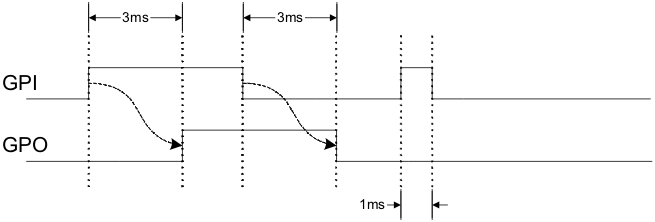
The GPOs can be configured so that they manifest a change in logic with a delay on assertion, deassertion, both or none. GPO behavior using delays will have different effects depending if the logic change occurs at a faster rate than the delay. On a normal delay configuration, if the logic for a GPO changes to a state and reverts back to previous state within the time of a delay then the GPO will not manifest the change of state on the pin. In Figure 7-15 the GPO is set so that it follows the GPI with a 3ms delay at assertion and also at de-assertion. When the GPI first changes to high logic state, the state is maintained for a time longer than the delay allowing the GPO to follow with appropriate logic state. The same goes for when the GPI returns to its previous low logic state. The second time that the GPI changes to a high logic state it returns to low logic state before the delay time expires. In this case the GPO does not change state. A delay configured in this manner serves as a glitch filter for the GPO.
 Figure 7-15 GPO Behavior When Not Ignoring Inputs During Delay
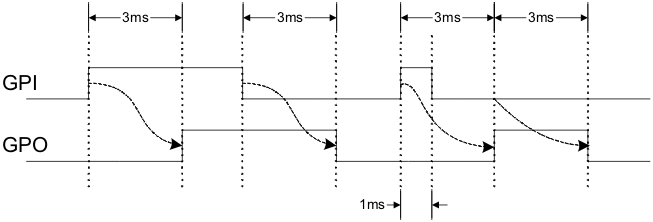
The Ignore Input During Delay bit allows to output a change in GPO even if it occurs for a time shorter than the delay. This configuration setting has the GPO ignore any activity from the triggering event until the delay expires. Figure 7-16 represents the two cases for when ignoring the inputs during a delay. In the case in which the logic changes occur with more time than the delay, the GPO signal looks the same as if the input was not ignored. Then on a GPI pulse shorter than the delay the GPO still changes state. Any pulse that occurs on the GPO when having the Ignore Input During Delay bit set will have a width of at least the time delay.
 Figure 7-16 GPO Behavior When Ignoring Inputs During Delay