SLVSC86A January 2014 – March 2014 UCD9244-EP
PRODUCTION DATA.
- 1 Features
- 2 Applications
- 3 Description
- 4 Revision History
- 5 Description (Continued)
- 6 Terminal Configuration and Functions
-
7 Specifications
- 7.1 Absolute Maximum Ratings
- 7.2 Handling Ratings
- 7.3 Recommended Operating Conditions
- 7.4 Thermal Information
- 7.5 Electrical Characteristics
- 7.6 Electrical Characteristics (Continued)
- 7.7 ADC Monitoring Intervals And Response Times
- 7.8 Hardware Fault Detection Latency
- 7.9 PMBus/SMBus/I2C
- 7.10 I2C/SMBus/PMBus Timing Requirements
- 7.11 Typical Characteristics
-
8 Detailed Description
- 8.1 Overview
- 8.2 Functional Block Diagram
- 8.3
Feature Description
- 8.3.1 PMBus Interface
- 8.3.2 Resistor Programmed PMBus Address Decode
- 8.3.3 VID Interface
- 8.3.4 Jtag Interface
- 8.3.5 Bias Supply Generator (Shunt Regulator Controller)
- 8.3.6 Power-On Reset
- 8.3.7 External Reset
- 8.3.8 ON_OFF_CONFIG
- 8.3.9 Output Voltage Adjustment
- 8.3.10 Calibration
- 8.3.11 Analog Front End (AFE)
- 8.3.12 Voltage Sense Filtering
- 8.3.13 DPWM Engine
- 8.3.14 Rail/Power Stage Configuration
- 8.3.15 DPWM Phase Synchronization
- 8.3.16 Output Current Measurement
- 8.3.17 Current Sense Input Filtering
- 8.3.18 Over-Current Detection
- 8.3.19 Input Voltage Monitoring
- 8.3.20 Input UV Lockout
- 8.3.21 Temperature Monitoring
- 8.3.22 Auxiliary ADC Input Monitoring
- 8.3.23 Soft Start, Soft Stop Ramp Sequence
- 8.3.24 Non-Volatile Memory Error Correction Coding
- 8.3.25 Data Logging
- 8.4 Device Functional Modes
- 9 Applications and Implementation
- 10Power Supply Recommendations
- 11Layout
- 12Device and Documentation Support
- 13Mechanical, Packaging, and Orderable Information
Package Options
Mechanical Data (Package|Pins)
- RGC|64
Thermal pad, mechanical data (Package|Pins)
- RGC|64
Orderable Information
8.3.11 Analog Front End (AFE)
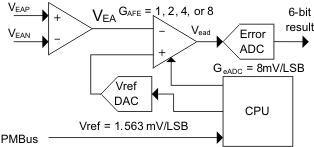
 Figure 8. Analog Front End Block Diagram
The UCD9244 senses the power supply output voltage differentially through the EAP and EAN terminals. The error amplifier utilizes a switched capacitor topology that provides a wide common mode range for the output voltage sense signals. The fully differential nature of the error amplifier also ensures low offset performance.
The output voltage is sampled at a programmable time (set by the EADC_SAMPLE_TRIGGER PMBus command). When the differential input voltage is sampled, the voltage is captured in internal capacitors and then transferred to the error amplifier where the value is subtracted from the set-point reference which is generated by the 10-bit Vref DAC as shown in Figure 8. The resulting error voltage is then amplified by a programmable gain circuit before the error voltage is converted to a digital value by the error ADC (EADC). This programmable gain is configured through the PMBus and affects the dynamic range and resolution of the sensed error voltage as shown in Table 2. The internal reference gains and offsets are factory-trimmed at the 4x gain setting, so it is recommended that this setting be used whenever possible.
Table 2. Analog Front End Resolution
| AFE_GAIN for PMBus Command | AFE Gain | EFFECTIVE ADC RESOLUTION (mV) | DIGITAL ERROR VOLTAGE DYNAMIC RANGE (mV) |
|---|---|---|---|
| 0 | 1x | 8 | –256 to 248 |
| 1 | 2x | 4 | –128 to 124 |
| 2 (Recommended) | 4x | 2 | –64 to 62 |
| 3 | 8x | 1 | –32 to 31 |
The AFE variable gain is one of the compensation coefficients that are stored when the device is configured by issuing the CLA_GAINS PMBus command. Compensator coefficients are arranged in several banks: one bank for start/stop ramp or tracking, one bank for normal regulation mode and one bank for light load mode. This allows the user to trade-off resolution and dynamic range for each operational mode.
The EADC, which samples the error voltage, has high accuracy, high resolution, and a fast conversion time. However, its range is limited as shown in Table 2. If the output voltage is different from the reference by more than this, the EADC reports a saturated value at –32 LSBs or 31 LSBs. The UCD9244 overcomes this limitation by adjusting the Vref DAC up or down in order to bring the error voltage out of saturation. In this way, the effective range of the ADC is extended. When the EADC saturates, the Vref DAC is slewed at a rate of 0.156 V/ms, referred to the EA differential inputs.
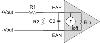
The differential feedback error voltage is defined as VEA = VEAP – VEAN. An attenuator network using resistors R1 and R2 (Figure 9) should be used to ensure that VEA does not exceed the maximum value of Vref when operating at the commanded voltage level. The commanded voltage level is determined by the PMBus settings described in the Output Voltage Adjustment section.
 Figure 9. Input Offset Equivalent Circuit