SLVSC86A January 2014 – March 2014 UCD9244-EP
PRODUCTION DATA.
- 1 Features
- 2 Applications
- 3 Description
- 4 Revision History
- 5 Description (Continued)
- 6 Terminal Configuration and Functions
-
7 Specifications
- 7.1 Absolute Maximum Ratings
- 7.2 Handling Ratings
- 7.3 Recommended Operating Conditions
- 7.4 Thermal Information
- 7.5 Electrical Characteristics
- 7.6 Electrical Characteristics (Continued)
- 7.7 ADC Monitoring Intervals And Response Times
- 7.8 Hardware Fault Detection Latency
- 7.9 PMBus/SMBus/I2C
- 7.10 I2C/SMBus/PMBus Timing Requirements
- 7.11 Typical Characteristics
-
8 Detailed Description
- 8.1 Overview
- 8.2 Functional Block Diagram
- 8.3
Feature Description
- 8.3.1 PMBus Interface
- 8.3.2 Resistor Programmed PMBus Address Decode
- 8.3.3 VID Interface
- 8.3.4 Jtag Interface
- 8.3.5 Bias Supply Generator (Shunt Regulator Controller)
- 8.3.6 Power-On Reset
- 8.3.7 External Reset
- 8.3.8 ON_OFF_CONFIG
- 8.3.9 Output Voltage Adjustment
- 8.3.10 Calibration
- 8.3.11 Analog Front End (AFE)
- 8.3.12 Voltage Sense Filtering
- 8.3.13 DPWM Engine
- 8.3.14 Rail/Power Stage Configuration
- 8.3.15 DPWM Phase Synchronization
- 8.3.16 Output Current Measurement
- 8.3.17 Current Sense Input Filtering
- 8.3.18 Over-Current Detection
- 8.3.19 Input Voltage Monitoring
- 8.3.20 Input UV Lockout
- 8.3.21 Temperature Monitoring
- 8.3.22 Auxiliary ADC Input Monitoring
- 8.3.23 Soft Start, Soft Stop Ramp Sequence
- 8.3.24 Non-Volatile Memory Error Correction Coding
- 8.3.25 Data Logging
- 8.4 Device Functional Modes
- 9 Applications and Implementation
- 10Power Supply Recommendations
- 11Layout
- 12Device and Documentation Support
- 13Mechanical, Packaging, and Orderable Information
Package Options
Mechanical Data (Package|Pins)
- RGC|64
Thermal pad, mechanical data (Package|Pins)
- RGC|64
Orderable Information
8.3.5 Bias Supply Generator (Shunt Regulator Controller)
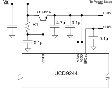
The I/O and analog circuits in the UCD9244 require 3.3V to operate. This can be provided using a stand-alone external 3.3V supply, or it can be generated from the main input supply using an internal shunt regulator and an external transistor. Regardless of which method is used to generate the 3.3V supply, bypass capacitors of 0.1 µF and 4.7 µF should be connected from V33A and V33D to ground near the device. An additional bypass capacitor from 0.1 to 1 µF must be connected from the BPCap terminal to ground for the internal 1.8V supply to the device’s logic circuits.
Figure 6 shows a typical application using the external transistor. The base of the transistor is driven by a resistor R1 to Vin and a transconductance amplifier whose output is on the V33FB terminal. The NPN emitter becomes the 3.3V supply for the chip.
 Figure 6. 3.3V Shunt Regulator Controller I/O
In order to generate the correct voltage on the base of the external pass transistor, the internal transconductance amplifier sinks current into the V33FB terminal and a voltage is produced across R1. This resistor value should be chosen so that ISINK is in the range from 0.2 to 0.4mA. R1 is defined as

Where ISINK is the current into the V33FB terminal; Vin is the power supply input voltage, typically 12V; IE is the current draw of the device and any pull up resistors tied to the 3.3V supply; and β is the beta of the pass transistor. For ISINK = 0.3 mA, Vin=12V, β=99, Vbe = 0.7V and IE=50mA, this formula selects R1 = 10kΩ. Weaker transistors or larger current loads will require less resistance to maintain the desired ISINK current. For example, lowering β to 40 would require R1 = 5.23 kΩ; likewise, an input voltage of 5V requires a value of 1.24 kΩ for R1.