SLVSC86A January 2014 – March 2014 UCD9244-EP
PRODUCTION DATA.
- 1 Features
- 2 Applications
- 3 Description
- 4 Revision History
- 5 Description (Continued)
- 6 Terminal Configuration and Functions
-
7 Specifications
- 7.1 Absolute Maximum Ratings
- 7.2 Handling Ratings
- 7.3 Recommended Operating Conditions
- 7.4 Thermal Information
- 7.5 Electrical Characteristics
- 7.6 Electrical Characteristics (Continued)
- 7.7 ADC Monitoring Intervals And Response Times
- 7.8 Hardware Fault Detection Latency
- 7.9 PMBus/SMBus/I2C
- 7.10 I2C/SMBus/PMBus Timing Requirements
- 7.11 Typical Characteristics
-
8 Detailed Description
- 8.1 Overview
- 8.2 Functional Block Diagram
- 8.3
Feature Description
- 8.3.1 PMBus Interface
- 8.3.2 Resistor Programmed PMBus Address Decode
- 8.3.3 VID Interface
- 8.3.4 Jtag Interface
- 8.3.5 Bias Supply Generator (Shunt Regulator Controller)
- 8.3.6 Power-On Reset
- 8.3.7 External Reset
- 8.3.8 ON_OFF_CONFIG
- 8.3.9 Output Voltage Adjustment
- 8.3.10 Calibration
- 8.3.11 Analog Front End (AFE)
- 8.3.12 Voltage Sense Filtering
- 8.3.13 DPWM Engine
- 8.3.14 Rail/Power Stage Configuration
- 8.3.15 DPWM Phase Synchronization
- 8.3.16 Output Current Measurement
- 8.3.17 Current Sense Input Filtering
- 8.3.18 Over-Current Detection
- 8.3.19 Input Voltage Monitoring
- 8.3.20 Input UV Lockout
- 8.3.21 Temperature Monitoring
- 8.3.22 Auxiliary ADC Input Monitoring
- 8.3.23 Soft Start, Soft Stop Ramp Sequence
- 8.3.24 Non-Volatile Memory Error Correction Coding
- 8.3.25 Data Logging
- 8.4 Device Functional Modes
- 9 Applications and Implementation
- 10Power Supply Recommendations
- 11Layout
- 12Device and Documentation Support
- 13Mechanical, Packaging, and Orderable Information
Package Options
Mechanical Data (Package|Pins)
- RGC|64
Thermal pad, mechanical data (Package|Pins)
- RGC|64
Orderable Information
8.3.15 DPWM Phase Synchronization
DPWM synchronization provides a method to link the timing between voltage rails controlled by the UCD92xx device--either internally or between devices. The configuration of the synchronization between rails is performed by the issuing the SYNC_CONFIG command. For details of issuing this command, see the UCD92xx PMBUS Command Reference (SLUU337). The synchronization behavior can also be configured using the Fusion Digital Power Designer software. Below is a summary of the function.
Each digital pulse width modulator (PWM) engine in the UCD92xx controller can accept a sync signal that resets the PWM ramp generator. The ramp generator can be set to free-run, accept a reset signal from another internal PWM engine, or accept a reset signal from the external SyncIn terminal. In this way the PWM timers can be "daisy-chained" to set up the desired phase relationship between power stages.
The PWM engine reset input can accept the following inputs
Table 3. Sync Trigger Inputs
| SYNC SIGNAL |
|---|
| None (free run) |
| DPWM 1 |
| DPWM 2 |
| DPWM 3 |
| DPWM 4 |
| SyncIn terminal |
Table 4. Available Source For SyncOut
| SYNC SIGNAL |
|---|
| Disabled |
| DPWM 1 |
| DPWM 2 |
| DPWM 3 |
| DPWM 4 |
When configuring a PWM engine to run synchronous to another internal PWM output, set the switching frequency of each PWM output to the same value using the FREQUENCY_SWITCH PMBus command. Set the time point where the controller samples the voltage to be regulated by setting the EADC_SAMPLE_TRIGGER value to the minimum value (228-240 nsec before the end of the switching period).
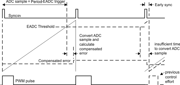
When configuring a PWM engine to run synchronous to an external sync signal, the switching period must be set to be longer than the period of the sync signal by setting the value of the FREQUENCY_SWITCH command to be lower than the frequency of the sync signal. This way the external sync signal will reset the PWM ramp counter before it is internally reset. In this operating condition, the error ADC sample trigger time must be set to:

where Fsw is the switching frequency set by FREQUENCY_SWITCH and Fsync is the minimum synchronization frequency. The factor of 0.95 is due to the 5% tolerance on the internal clock in the controller. This will ensure that the regulation voltage is sampled "just in time" to calculate the appropriate control effort for each switching period. This is shown in Figure 11.
 Figure 11. Relationship Of EADC Trigger To External Sync
If two rails share a common sync source other than the SyncIn terminal, they must have the same delay. When the SyncIn terminal is used as a sync source, the delay is applied using a different register (EV1) than when using the other sources (which use the PhaseTrig registers). Using the EV1 register introduces delay in the control loop calculation that will introduce phase loss that must be taken into consideration when calculating the loop compensation. Therefore, under most conditions it will be desirable to set the delay to zero for the PWM signal synchronized by the SyncIn terminal.