SLVSC86A January 2014 – March 2014 UCD9244-EP
PRODUCTION DATA.
- 1 Features
- 2 Applications
- 3 Description
- 4 Revision History
- 5 Description (Continued)
- 6 Terminal Configuration and Functions
-
7 Specifications
- 7.1 Absolute Maximum Ratings
- 7.2 Handling Ratings
- 7.3 Recommended Operating Conditions
- 7.4 Thermal Information
- 7.5 Electrical Characteristics
- 7.6 Electrical Characteristics (Continued)
- 7.7 ADC Monitoring Intervals And Response Times
- 7.8 Hardware Fault Detection Latency
- 7.9 PMBus/SMBus/I2C
- 7.10 I2C/SMBus/PMBus Timing Requirements
- 7.11 Typical Characteristics
-
8 Detailed Description
- 8.1 Overview
- 8.2 Functional Block Diagram
- 8.3
Feature Description
- 8.3.1 PMBus Interface
- 8.3.2 Resistor Programmed PMBus Address Decode
- 8.3.3 VID Interface
- 8.3.4 Jtag Interface
- 8.3.5 Bias Supply Generator (Shunt Regulator Controller)
- 8.3.6 Power-On Reset
- 8.3.7 External Reset
- 8.3.8 ON_OFF_CONFIG
- 8.3.9 Output Voltage Adjustment
- 8.3.10 Calibration
- 8.3.11 Analog Front End (AFE)
- 8.3.12 Voltage Sense Filtering
- 8.3.13 DPWM Engine
- 8.3.14 Rail/Power Stage Configuration
- 8.3.15 DPWM Phase Synchronization
- 8.3.16 Output Current Measurement
- 8.3.17 Current Sense Input Filtering
- 8.3.18 Over-Current Detection
- 8.3.19 Input Voltage Monitoring
- 8.3.20 Input UV Lockout
- 8.3.21 Temperature Monitoring
- 8.3.22 Auxiliary ADC Input Monitoring
- 8.3.23 Soft Start, Soft Stop Ramp Sequence
- 8.3.24 Non-Volatile Memory Error Correction Coding
- 8.3.25 Data Logging
- 8.4 Device Functional Modes
- 9 Applications and Implementation
- 10Power Supply Recommendations
- 11Layout
- 12Device and Documentation Support
- 13Mechanical, Packaging, and Orderable Information
Package Options
Mechanical Data (Package|Pins)
- RGC|64
Thermal pad, mechanical data (Package|Pins)
- RGC|64
Orderable Information
8.3.3 VID Interface
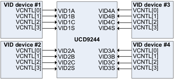
The UCD9244 supports VID (Voltage Identification) inputs from up to four external VID enabled devices. The VID codes may be 4-, 6-, or 8-bit values; the format is selected using the VID_CONFIG PMBus command. In 4- and 6-bit mode, each host uses four VID input signals (VID_A, VID_B, VID_C, and VID_S) to send VID codes to the UCD9244. In 8-bit mode, the PMBus input is used to receive VID commands from the VID devices’ I2C interfaces.

Regardless of which VID mode is used, the commanded output voltage reference is set according to this formula:
where
and
The VID_Vout_High, VID_Vout_Low, and VID_Format values are set using the VID_CONFIG PMBus command. The same command is used to set the initial VID code that will be used at power-up. In addition, the VID_CONFIG command also sets the initial voltage that the device ramps to at the end of the soft start; and defines a lockout interval over which the VID is ignored during the soft start.
VID Lockout Interval: Because the VID signals may be originating from a device that is being powered by the UCD9244, the voltage levels on the VID signal may not be valid logic levels until the supply voltage at the powered device has stabilized. For this reason a configurable lockout interval is applied each time the regulated output voltage is turned on. The lockout interval timer starts when the output voltage reaches the top of the soft-start ramp. Positive values range from 1 to 32767 ms, with 1 ms resolution. A value of 0 will enable the VID inputs immediately at the top of the start ramp. Negative values disable the lockout, allowing the VID inputs to remain active all the time regardless of the output voltage state. The default value is 0.