SLRS059B April 2012 – June 2015 ULN2003LV
PRODUCTION DATA.
- 1 Features
- 2 Applications
- 3 Description
- 4 Revision History
- 5 Pin Configuration and Functions
- 6 Specifications
- 7 Detailed Description
- 8 Application and Implementation
- 9 Power Supply Recommendations
- 10Layout
- 11Device and Documentation Support
- 12Mechanical, Packaging, and Orderable Information
Package Options
Mechanical Data (Package|Pins)
Thermal pad, mechanical data (Package|Pins)
Orderable Information
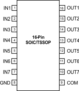
5 Pin Configuration and Functions
D or PW Package
16-Pin SOIC or TSSOP
Top View

Pin Functions
| PIN | TYPE | DESCRIPTION | |
|---|---|---|---|
| NAME | NO. | ||
| IN1 | 1 | Input | Logic Input Pins IN1 through IN7 |
| IN2 | 2 | Input | |
| IN3 | 3 | Input | |
| IN4 | 4 | Input | |
| IN5 | 5 | Input | |
| IN6 | 6 | Input | |
| IN7 | 7 | Input | |
| GND | 8 | Ground | Ground Reference Pin |
| COM | 9 | Output | Internal Free-Wheeling Diode Common Cathode Pin |
| OUT7 | 10 | Output | Channel Output Pins OUT7 through OUT1 |
| OUT6 | 11 | Output | |
| OUT5 | 12 | Output | |
| OUT4 | 13 | Output | |
| OUT3 | 14 | Output | |
| OUT2 | 15 | Output | |
| OUT1 | 16 | Output | |