SLRS027S December 1976 – June 2024 ULN2002A , ULN2003A , ULN2003AI , ULN2004A , ULQ2003A , ULQ2004A
PRODUCTION DATA
- 1
- 1 Features
- 2 Applications
- 3 Description
- 4 Pin Configuration and Functions
-
5 Specifications
- 5.1 Absolute Maximum Ratings
- 5.2 ESD Ratings
- 5.3 Recommended Operating Conditions
- 5.4 Thermal Information
- 5.5 Electrical Characteristics: ULN2002A
- 5.6 Electrical Characteristics: ULN2003A and ULN2004A
- 5.7 Electrical Characteristics: ULN2003AI
- 5.8 Electrical Characteristics: ULN2003AI
- 5.9 Electrical Characteristics: ULQ2003A and ULQ2004A
- 5.10 Switching Characteristics: ULN2002A, ULN2003A, ULN2004A
- 5.11 Switching Characteristics: ULN2003AI
- 5.12 Switching Characteristics: ULN2003AI
- 5.13 Switching Characteristics: ULQ2003A, ULQ2004A
- 5.14 Typical Characteristics
- 6 Parameter Measurement Information
- 7 Detailed Description
- 8 Application and Implementation
- 9 Device and Documentation Support
- 10Revision History
- 11Mechanical, Packaging, and Orderable Information
Package Options
Refer to the PDF data sheet for device specific package drawings
Mechanical Data (Package|Pins)
- NS|16
- N|16
- D|16
Thermal pad, mechanical data (Package|Pins)
Orderable Information
6 Parameter Measurement Information
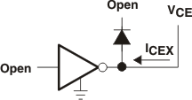 Figure 6-1 ICEX Test Circuit
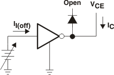 Figure 6-3 II(off) Test Circuit
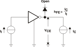
II is fixed for measuring VCE(sat), variable
for measuring hFE.
Figure 6-5 hFE, VCE(sat) Test Circuit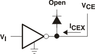 Figure 6-2 ICEX Test Circuit
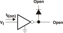 Figure 6-4 II Test Circuit
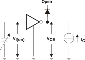 Figure 6-6 VI(on) Test Circuit
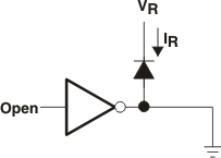 Figure 6-7 IR Test Circuit
 Figure 6-8 VF Test Circuit
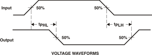 Figure 6-9 Propagation Delay-Time Waveforms
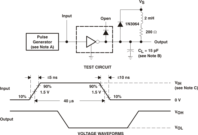
The pulse
generator has the following characteristics: PRR = 12.5 kHz,
ZO = 50 Ω.
CL includes probe and jig capacitance.
For
testing the ULN2003A device, ULN2003AI device, and ULQ2003A devices,
VIH = 3 V; for the ULN2002A device, VIH = 13
V; for the ULN2004A and the ULQ2004A devices, VIH = 8
V.
Figure 6-10 Latch-Up Test Circuit and Voltage Waveforms