SLRS027S December 1976 – June 2024 ULN2002A , ULN2003A , ULN2003AI , ULN2004A , ULQ2003A , ULQ2004A
PRODUCTION DATA
- 1
- 1 Features
- 2 Applications
- 3 Description
- 4 Pin Configuration and Functions
-
5 Specifications
- 5.1 Absolute Maximum Ratings
- 5.2 ESD Ratings
- 5.3 Recommended Operating Conditions
- 5.4 Thermal Information
- 5.5 Electrical Characteristics: ULN2002A
- 5.6 Electrical Characteristics: ULN2003A and ULN2004A
- 5.7 Electrical Characteristics: ULN2003AI
- 5.8 Electrical Characteristics: ULN2003AI
- 5.9 Electrical Characteristics: ULQ2003A and ULQ2004A
- 5.10 Switching Characteristics: ULN2002A, ULN2003A, ULN2004A
- 5.11 Switching Characteristics: ULN2003AI
- 5.12 Switching Characteristics: ULN2003AI
- 5.13 Switching Characteristics: ULQ2003A, ULQ2004A
- 5.14 Typical Characteristics
- 6 Parameter Measurement Information
- 7 Detailed Description
- 8 Application and Implementation
- 9 Device and Documentation Support
- 10Revision History
- 11Mechanical, Packaging, and Orderable Information
Package Options
Refer to the PDF data sheet for device specific package drawings
Mechanical Data (Package|Pins)
- N|16
- D|16
Thermal pad, mechanical data (Package|Pins)
Orderable Information
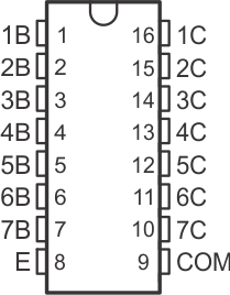
4 Pin Configuration and Functions
 Figure 4-1 D, N, NS, and PW Package16-Pin SOIC,
PDIP, SO, and TSSOPTop View
Figure 4-1 D, N, NS, and PW Package16-Pin SOIC,
PDIP, SO, and TSSOPTop ViewTable 4-1 Pin Functions
| PIN | I/O(1) | DESCRIPTION | |
|---|---|---|---|
| NAME | NO. | ||
| 1B | 1 | I | Channel 1 through 7 Darlington base input |
| 2B | 2 | ||
| 3B | 3 | ||
| 4B | 4 | ||
| 5B | 5 | ||
| 6B | 6 | ||
| 7B | 7 | ||
| 1C | 16 | O | Channel 1 through 7 Darlington collector output |
| 2C | 15 | ||
| 3C | 14 | ||
| 4C | 13 | ||
| 5C | 12 | ||
| 6C | 11 | ||
| 7C | 10 | ||
| COM | 9 | — | Common cathode node for flyback diodes (required for inductive loads) |
| E | 8 | — | Common emitter shared by all channels (typically tied to ground) |
(1) I = Input, O = Output