SLRS027S December 1976 – June 2024 ULN2002A , ULN2003A , ULN2003AI , ULN2004A , ULQ2003A , ULQ2004A
PRODUCTION DATA
- 1
- 1 Features
- 2 Applications
- 3 Description
- 4 Pin Configuration and Functions
-
5 Specifications
- 5.1 Absolute Maximum Ratings
- 5.2 ESD Ratings
- 5.3 Recommended Operating Conditions
- 5.4 Thermal Information
- 5.5 Electrical Characteristics: ULN2002A
- 5.6 Electrical Characteristics: ULN2003A and ULN2004A
- 5.7 Electrical Characteristics: ULN2003AI
- 5.8 Electrical Characteristics: ULN2003AI
- 5.9 Electrical Characteristics: ULQ2003A and ULQ2004A
- 5.10 Switching Characteristics: ULN2002A, ULN2003A, ULN2004A
- 5.11 Switching Characteristics: ULN2003AI
- 5.12 Switching Characteristics: ULN2003AI
- 5.13 Switching Characteristics: ULQ2003A, ULQ2004A
- 5.14 Typical Characteristics
- 6 Parameter Measurement Information
- 7 Detailed Description
- 8 Application and Implementation
- 9 Device and Documentation Support
- 10Revision History
- 11Mechanical, Packaging, and Orderable Information
Package Options
Refer to the PDF data sheet for device specific package drawings
Mechanical Data (Package|Pins)
- N|16
- D|16
Thermal pad, mechanical data (Package|Pins)
Orderable Information
8.2.2.3 Power Dissipation and Temperature
The number of coils driven is dependent on the coil current and on-chip power dissipation. The number of coils driven can be determined by Figure 5-4 or Figure 5-5.
For a more accurate determination of number of coils possible, use the below equation to calculate ULN2003A device on-chip power dissipation PD:
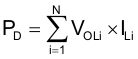
where
- N is the number of channels active together
- VOLi is the OUTi pin voltage for the load current ILi. This is the same as VCE(SAT)
To ensure reliability of ULN2003A device and the system, the on-chip power dissipation must be lower that or equal to the maximum allowable power dissipation (PD(MAX)) dictated by below equation Equation 3.
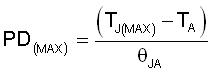
where
- TJ(max) is the target maximum junction temperature
- TA is the operating ambient temperature
- RθJA is the package junction to ambient thermal resistance
Limit the die junction temperature of the ULN2003A device to less than 125°C. The IC junction temperature is directly proportional to the on-chip power dissipation.