SWRS170K March 2014 – November 2023 WL1807MOD , WL1837MOD
PRODUCTION DATA
- 1
- 1 Features
- 2 Applications
- 3 Description
- 4 Functional Block Diagram
- 5 Revision History
- 6 Device Comparison
- 7 Terminal Configuration and Functions
-
8 Specifications
- 8.1 Absolute Maximum Ratings
- 8.2 ESD Ratings
- 8.3 Recommended Operating Conditions
- 8.4 External Digital Slow Clock Requirements
- 8.5 Thermal Resistance Characteristics for MOC 100-Pin Package
- 8.6 WLAN Performance: 2.4-GHz Receiver Characteristics
- 8.7 WLAN Performance: 2.4-GHz Transmitter Power
- 8.8 WLAN Performance: 5-GHz Receiver Characteristics
- 8.9 WLAN Performance: 5-GHz Transmitter Power
- 8.10 WLAN Performance: Currents
- 8.11 Bluetooth Performance: BR, EDR Receiver Characteristics—In-Band Signals
- 8.12 Bluetooth Performance: Transmitter, BR
- 8.13 Bluetooth Performance: Transmitter, EDR
- 8.14 Bluetooth Performance: Modulation, BR
- 8.15 Bluetooth Performance: Modulation, EDR
- 8.16 Bluetooth low energy Performance: Receiver Characteristics – In-Band Signals
- 8.17 Bluetooth low energy Performance: Transmitter Characteristics
- 8.18 Bluetooth low energy Performance: Modulation Characteristics
- 8.19 Bluetooth BR and EDR Dynamic Currents
- 8.20 Bluetooth low energy Currents
- 8.21
Timing and Switching Characteristics
- 8.21.1 Power Management
- 8.21.2 Power-Up and Shut-Down States
- 8.21.3 Chip Top-level Power-Up Sequence
- 8.21.4 WLAN Power-Up Sequence
- 8.21.5 Bluetooth-Bluetooth low energy Power-Up Sequence
- 8.21.6 WLAN SDIO Transport Layer
- 8.21.7 HCI UART Shared-Transport Layers for All Functional Blocks (Except WLAN)
- 8.21.8 Bluetooth Codec-PCM (Audio) Timing Specifications
- 9 Detailed Description
- 10Applications, Implementation, and Layout
- 11Device and Documentation Support
- 12Mechanical, Packaging, and Orderable Information
Package Options
Refer to the PDF data sheet for device specific package drawings
Mechanical Data (Package|Pins)
- MOC|100
Thermal pad, mechanical data (Package|Pins)
Orderable Information
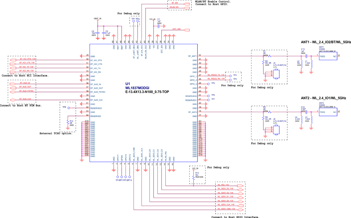
10.1.1 Typical Application – WL1837MOD Reference Design
Figure 10-1 shows the TI WL1837MODGI reference design.
 Figure 10-1 TI Module Reference Schematics
Table 10-1 lists the bill materials (BOM).
Table 10-1 Bill of Materials
| ITEM | DESCRIPTION | PART NO. | PACKAGE | REFERENCE | QTY | MFR |
|---|---|---|---|---|---|---|
| 1 | WL1837 Wi-Fi / Bluetooth module | WL1837MODGI | 13.4 × 13.3 × 2.0 mm | U1 | 1 | TI |
| 2 | XOSC 3225 / 32.768 kHz / 1.8 V / ±50 ppm | 7XZ3200005 | 3.2 × 2.5 × 1.0 mm | OSC1 | 1 | TXC |
| 3 | ANT / Chip / 2.4 GHz and 5 GHz(1) | W3006 | 10.0 × 3.2 × 1.5 mm | ANT1, ANT2 | 2 | Pulse |
| 4 | Mini-RF header receptacle | U.FL-R-SMT-1 (10) | 3.0 × 2.6 × 1.25 mm | J5, J6 | 2 | Hirose |
| 5 | Inductor 0402 / 1.3 nH / ±0.1 nH / SMD | LQP15MN1N3B02 | 0402 | L1 | 1 | Murata |
| 6 | Inductor 0402 / 1.8 nH / ±0.1 nH / SMD | LQP15MN1N8B02 | 0402 | L3 | 1 | Murata |
| 7 | Inductor 0402 / 2.2 nH / ±0.1 nH / SMD | LQP15MN2N2B02 | 0402 | L4 | 1 | Murata |
| 8 | Capacitor 0402 / 1 pF/ 50 V / C0G / ±0.1 pF | GJM1555C1H1R0BB01 | 0402 | C13 | 1 | Murata |
| 9 | Capacitor 0402 / 2.4 pF / 50 V / C0G / ±0.1 pF | GJM1555C1H2R4BB01 | 0402 | C14 | 1 | Murata |
| 10 | Capacitor 0402 / 0.1 µF / 10 V / X7R / ±10% | 0402B104K100CT | 0402 | C3 | 1 | Walsin |
| 11 | Capacitor 0402 / 1 µF / 6.3 V / X5R / ±10%/HF | GRM155R60J105KE19D | 0402 | C1 | 1 | Murata |
| 12 | Capacitor 0603 / 10 µF / 6.3 V / X5R / ±20% | C1608X5R0J106M | 0603 | C2 | 1 | TDK |
| 13 | Resistor 0402 / 0R / ±5% | WR04X000 PTL | 0402 | R1, R3 | 2 | Walsin |
(1) For more information, see the Pulse Electronics W3006 product page.