SBOS061C February   1997  – October 2024 XTR105

PRODUCTION DATA  

  1.   1
  2. Features
  3. Applications
  4. Description
  5. Pin Configuration and Functions
  6. Specifications
    1. 5.1 Absolute Maximum Ratings #GUID-80F0CD5F-C345-42B2-B6A9-580512790460/R_DESCRIPTION_LI1
    2. 5.2 Recommended Operating Conditions
    3. 5.3 Thermal Information
    4. 5.4 Electrical Characteristics
    5. 5.5 Typical Characteristics
  7. Detailed Description
    1. 6.1 Overview
    2. 6.2 Functional Block Diagram
    3. 6.3 Feature Description
      1. 6.3.1 Linearization
        1. 6.3.1.1 High-Resistance RTDs
      2. 6.3.2 Voltage Regulator
      3. 6.3.3 Open-Circuit Protection
      4. 6.3.4 Reverse-Voltage Protection
      5. 6.3.5 Surge Protection
    4. 6.4 Device Functional Modes
  8. Application and Implementation
    1. 7.1 Application Information
      1. 7.1.1 External Transistor
      2. 7.1.2 Loop Power Supply
      3. 7.1.3 2-Wire and 3-Wire RTD Connections
      4. 7.1.4 Radio Frequency Interference
      5. 7.1.5 Error Analysis
    2. 7.2 Typical Applications
    3. 7.3 Layout
      1. 7.3.1 Layout Guidelines
  9. Device and Documentation Support
    1. 8.1 Documentation Support
      1. 8.1.1 Related Documentation
    2. 8.2 Receiving Notification of Documentation Updates
    3. 8.3 Support Resources
    4. 8.4 Trademarks
    5. 8.5 Electrostatic Discharge Caution
    6. 8.6 Glossary
  10. Revision History
  11. 10Mechanical, Packaging, and Orderable Information

Package Options

Refer to the PDF data sheet for device specific package drawings

Mechanical Data (Package|Pins)
  • D|14
  • N|14
Thermal pad, mechanical data (Package|Pins)
Orderable Information

Voltage Regulator

The VREG pin provides an on-chip voltage source of approximately 5.1V and is designed for powering external input circuitry (as shown in Figure 6-2). This source is a moderately accurate voltage reference, and is not the same reference used to set the 800µA current references. VREG is capable of sourcing approximately 1mA of current. Exceeding 1mA can affect the 4mA zero output.
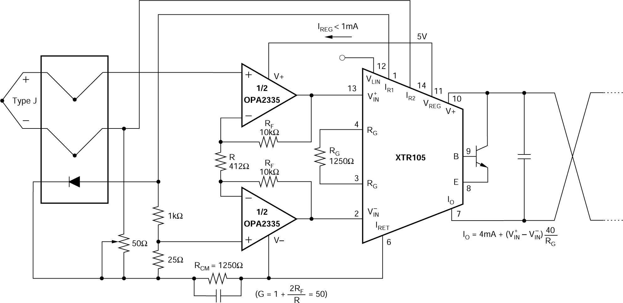
XTR105 Thermocouple Low Offset, Low
                    Drift Loop Measurement With Diode Cold Junction Compensation Figure 6-2 Thermocouple Low Offset, Low Drift Loop Measurement With Diode Cold Junction Compensation