SBOS061C February 1997 – October 2024 XTR105
PRODUCTION DATA
- 1
- 1 Features
- 2 Applications
- 3 Description
- 4 Pin Configuration and Functions
- 5 Specifications
- 6 Detailed Description
- 7 Application and Implementation
- 8 Device and Documentation Support
- 9 Revision History
- 10Mechanical, Packaging, and Orderable Information
Package Options
Refer to the PDF data sheet for device specific package drawings
Mechanical Data (Package|Pins)
- D|14
- N|14
Thermal pad, mechanical data (Package|Pins)
Orderable Information
6.1 Overview
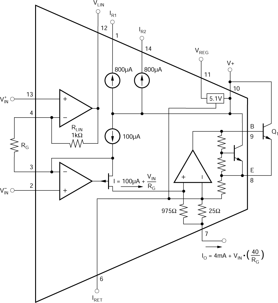
The XTR105 is a monolithic 4mA-to-20mA, 2-wire current transmitter with a differential voltage input. Figure 6-1 shows the simplified schematic of the XTR105. The loop power supply, V+, provides power for all circuitry. The output loop current is modulated by the XTR105 and is typically measured as a voltage across a series load resistor (RL).
The instrumentation amplifier input of the XTR105 measures the voltage difference between the noninverting and inverting inputs. This difference is then gained up according to the value of RG, and expressed as a regulated current output.
The two matched 0.8mA current sources are typically used to drive an RTD and zero-setting resistor (RZ). RZ determines the static offset of the current output and can be adjusted to correct for offset errors. A linearity correction feature is provided to further improve the RTD response. An additional 5.1V voltage regulator output is provided to power external circuitry such as buffer amplifiers.
 Figure 6-1 Simplified Schematic