SBOS375D October 2006 – October 2024 XTR111
PRODUCTION DATA
- 1
- 1 Features
- 2 Applications
- 3 Description
- 4 Pin Configurations and Functions
- 5 Specifications
- 6 Detailed Description
- 7 Application and Implementation
- 8 Device and Documentation Support
- 9 Revision History
- 10Mechanical, Packaging, and Orderable Information
Package Options
Refer to the PDF data sheet for device specific package drawings
Mechanical Data (Package|Pins)
- DRC|10
- DGQ|10
Thermal pad, mechanical data (Package|Pins)
Orderable Information
6.1 Overview
The XTR111 is a voltage-controlled current source capable of delivering currents from 0mA to 32mA. The primary intent of the XTR111 is to source the commonly-used industrial current ranges of 0mA to 20mA or 4mA to 20mA. The performance is specified for a supply voltage of up to 40V. The maximum supply voltage is 44V. The voltage-to-current ratio is defined by an external resistor, RSET; therefore, the input voltage range can be freely set in accordance with application requirements. The output current is cascoded by an external P-channel MOSFET transistor for large voltage compliance extending below ground, and for easy power dissipation. This arrangement provides excellent suppression of typical interference signals from the industrial environment because of the extremely high output impedance and wide voltage compliance.
An error detection circuit activates a logic output (error flag pin, EF) in case the output current cannot correctly flow. The EF pin indicates a wire break, high load resistor, or loss of headroom for the current output to the positive supply. The output disable (OD) pin provided can be used during power-on, multiplexing, and other conditions where the output presents no current. The OD pin has an internal pullup that causes the XTR111 to come up in output disable mode unless the OD pin is tied low.
The onboard voltage regulator can be adjusted from 3V to 15V and delivers up to 5mA load current. The voltage regulator is intended to supply signal conditioning and sensor excitation in 3-wire sensor systems. Voltages greater than 3V can be set by a resistive divider.
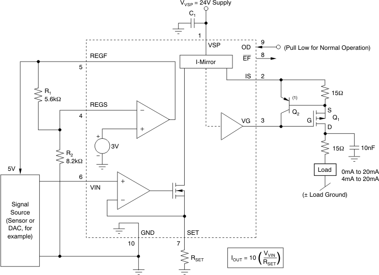
Figure 6-1 shows the basic connections. Input voltage VVIN reappears across RSET and controls 1/10 of the output current. The I-Mirror has a precise current gain of 10. This configuration has a transfer function of:
Set the voltage regulator output to a range of 3V to 12V by selecting R1 and R2 using the following equation:
 Figure 6-1 Basic Connection for 0mA to
20mA Related to a 0V-to-5V Signal Input With the Voltage Regulator Set to a 5V
Output