SBOS375D October   2006  – October 2024 XTR111

PRODUCTION DATA  

  1.   1
  2. Features
  3. Applications
  4. Description
  5. Pin Configurations and Functions
  6. Specifications
    1. 5.1 Absolute Maximum Ratings
    2. 5.2 ESD Ratings
    3. 5.3 Recommended Operating Conditions
    4. 5.4 Thermal Information
    5. 5.5 Electrical Characteristics
    6. 5.6 Typical Characteristics
  7. Detailed Description
    1. 6.1 Overview
    2. 6.2 Functional Block Diagram
    3. 6.3 Feature Description
      1. 6.3.1 Explanation of Pin Functions
      2. 6.3.2 Dynamic Performance
      3. 6.3.3 External Current Limit
      4. 6.3.4 External MOSFET
      5. 6.3.5 Output Error Flag and Disable Input
      6. 6.3.6 Voltage Regulator
      7. 6.3.7 Level Shift of 0V Input and Transconductance Trim
    4. 6.4 Device Functional Modes
  8. Application and Implementation
    1. 7.1 Application Information
      1. 7.1.1 Input Voltage
      2. 7.1.2 Error Flag Delay
      3. 7.1.3 Voltage Output Configuration
      4. 7.1.4 4mA-to-20mA Output
    2. 7.2 Typical Applications
      1. 7.2.1 0mA–20mA Voltage-to-Current Converter
        1. 7.2.1.1 Design Requirements
        2. 7.2.1.2 Detailed Design Procedure
        3. 7.2.1.3 Application Curve
      2. 7.2.2 Additional Applications
    3. 7.3 Power Supply Recommendations
    4. 7.4 Layout
      1. 7.4.1 Layout Guidelines
        1. 7.4.1.1 Package and Heat Dissipation
        2. 7.4.1.2 Thermal Pad Guidelines
      2. 7.4.2 Layout Example
  9. Device and Documentation Support
    1. 8.1 Device Support
      1. 8.1.1 Third-Party Products Disclaimer
    2. 8.2 Documentation Support
      1. 8.2.1 Related Documentation
    3. 8.3 Receiving Notification of Documentation Updates
    4. 8.4 Support Resources
    5. 8.5 Trademarks
    6. 8.6 Electrostatic Discharge Caution
    7. 8.7 Glossary
  10. Revision History
  11. 10Mechanical, Packaging, and Orderable Information

Package Options

Refer to the PDF data sheet for device specific package drawings

Mechanical Data (Package|Pins)
  • DRC|10
  • DGQ|10
Thermal pad, mechanical data (Package|Pins)
Orderable Information

Dynamic Performance

The rise time of the output current is dominated by the gate capacitance of the external FET.

The accuracy of the current mirror relies on the dynamic matching of multiple individual current sources. Settling to full resolution can require a complete cycle lasting around 100μs. Figure 6-2 shows an example of the ripple generated from the individual current source values that average to the specified accuracy over the full cycle.
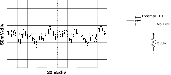
XTR111 Output Noise Without Filter
                    Into 500Ω Figure 6-2 Output Noise Without Filter Into 500Ω

The output glitch magnitude depends on the mismatch of the internal current sources. The output glitch magnitude is approximately proportional to the output current level and scales directly with the load resistor value. The output glitch magnitude differs slightly from device to device. Figure 6-3 and Figure 6-4 show the effects of filtering the output.
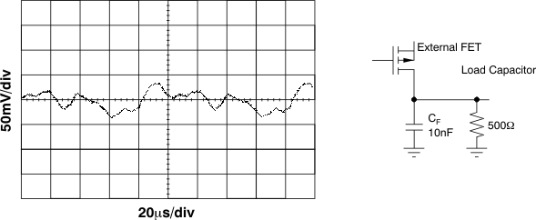
XTR111 Output With 10nF Parallel to
                    500Ω Figure 6-3 Output With 10nF Parallel to 500Ω
XTR111 Output With Additional
                    Filter Figure 6-4 Output With Additional Filter