-
ADS1018-Q1 Automotive, Low-Power, SPI™-Compatible, 12-Bit, Analog-to-Digital Converter With Internal Reference and Temperature Sensor
- 1 Features
- 2 Applications
- 3 Description
- 4 Revision History
- 5 Device Comparison Table
- 6 Pin Configuration and Functions
- 7 Specifications
- 8 Detailed Description
- 9 Application and Implementation
- 10Power Supply Recommendations
- 11Layout
- 12Device and Documentation Support
- 13Mechanical, Packaging, and Orderable Information
- IMPORTANT NOTICE
Package Options
Mechanical Data (Package|Pins)
- DGS|10
Thermal pad, mechanical data (Package|Pins)
Orderable Information
ADS1018-Q1 Automotive, Low-Power, SPI™-Compatible, 12-Bit, Analog-to-Digital Converter With Internal Reference and Temperature Sensor
1 Features
- AEC-Q100 qualified for automotive applications:
- Temperature grade 1: –40°C to +125°C, TA
- Functional Safety-Capable
- 12-bit noise-free resolution
- Wide supply range: 2 V to 5.5 V
- Low current consumption:
- Continuous mode: only 150 μA
- Single-shot mode: automatic power-down
- Programmable data rate: 128 SPS to 3300 SPS
- Single-cycle settling
- Internal low-drift voltage reference
- Internal temperature sensor:
2°C (maximum) error - Internal oscillator
- Internal PGA
- Four single-ended or two differential inputs
2 Applications
- Battery management systems
- Automotive sensors:
- Thermocouples
- Resistance temperature detectors (RTDs)
- Electrochemical gas sensors
- Particulate matter sensors
3 Description
The ADS1018-Q1 is a precision, low power, 12-bit, noise-free, analog-to-digital converter (ADC) that provides all features necessary to measure the most common sensor signals. The ADS1018-Q1 integrates a programmable gain amplifier (PGA), voltage reference, oscillator, and high-accuracy temperature sensor. These features, along with a wide power-supply range from 2 V to 5.5 V, make the
ADS1018-Q1 ideally suited for power- and space-constrained, sensor-measurement applications.
The ADS1018-Q1 performs conversions at data rates up to 3300 samples per second (SPS). The PGA offers input ranges from ±256 mV to ±6.144 V, allowing both large and small signals to be measured with high resolution. An input multiplexer (mux) allows measurement of two differential or four single-ended inputs. The high-accuracy temperature sensor is used for system-level temperature monitoring, or cold-junction compensation for thermocouples.
The ADS1018-Q1 operates either in continuous-conversion mode, or in a single-shot mode that automatically powers down after a conversion. Single-shot mode significantly reduces current consumption during idle periods. Data are transferred through a serial peripheral interface (SPI™). The ADS1018-Q1 is specified from –40°C to +125°C.
Device Information(1)
| PART NUMBER | PACKAGE | BODY SIZE (NOM) |
|---|---|---|
| ADS1018-Q1 | VSSOP (10) | 3.00 mm × 3.00 mm |
- For all available packages, see the package option addendum at the end of the data sheet.
Device Images
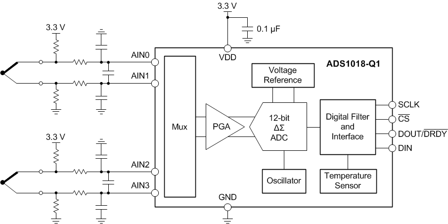
K-Type Thermocouple Measurement
Using Integrated Temperature Sensor for Cold-Junction Compensation

4 Revision History
Changes from A Revision (November 2015) to B Revision
- Changed automotive-specific Features bullets, moved ESD information to ESD Ratings table Go
- Added Functional Safety-Capable bullets to Features sectionGo
- Changed maximum VDD voltage from 5.5 V to 7 V in the Absolute Maximum Ratings tableGo
- Added ESD classification information to ESD Ratings table Go
- Changed maximum value of tSPWL parameter in Timing Requirements table from 28 ms to 30.8 msGo
- Changed SCLK low time to reset SPI from 28 ms to 30.8 ms in second footnote ofTiming Requirements tableGo
- Changed Serial Interface Timing figureGo
- Changed SCLK low time to reset SPI from 28 ms to 30.8 ms in the Serial Clock sectionGo
- Added last paragraph to the 32-Bit Data Transmission Cycle sectionGo
- Changed bit description of Config Register bit 0Go
- Changed SCLK low time to reset SPI from 28 ms to 30.8 ms in the GPIO Ports for Communication sectionGo
Changes from * Revision (October 2015) to A Revision
- Changed from product preview to production dataGo
5 Device Comparison Table
| DEVICE | RESOLUTION
(Bits) |
MAXIMUM SAMPLE RATE
(SPS) |
INPUT CHANNELS
Differential (Single-Ended) |
PGA | INTERFACE | SPECIAL FEATURES |
|---|---|---|---|---|---|---|
| ADS1118-Q1 | 16 | 860 | 2 (4) | Yes | SPI | Temperature sensor |
| ADS1018-Q1 | 12 | 3300 | 2 (4) | Yes | SPI | Temperature sensor |
| ADS1115-Q1 | 16 | 860 | 2 (4) | Yes | I2C | Comparator |
| ADS1015-Q1 | 12 | 3300 | 2 (4) | Yes | I2C | Comparator |
6 Pin Configuration and Functions

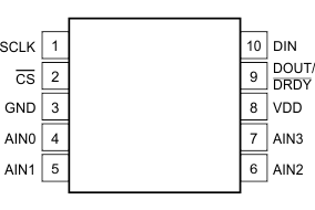
Pin Functions
| PIN | TYPE | DESCRIPTION | |
|---|---|---|---|
| NO. | NAME | ||
| 1 | SCLK | Digital input | Serial clock input |
| 2 | CS | Digital input | Chip select; active low. Connect to GND if not used. |
| 3 | GND | Supply | Ground |
| 4 | AIN0 | Analog input | Analog input 0. Leave unconnected or tie to VDD if not used. |
| 5 | AIN1 | Analog input | Analog input 1. Leave unconnected or tie to VDD if not used. |
| 6 | AIN2 | Analog input | Analog input 2. Leave unconnected or tie to VDD if not used. |
| 7 | AIN3 | Analog input | Analog input 3. Leave unconnected or tie to VDD if not used. |
| 8 | VDD | Supply | Power supply. Connect a 0.1-µF power supply decoupling capacitor to GND. |
| 9 | DOUT/DRDY | Digital output | Serial data output combined with data ready; active low |
| 10 | DIN | Digital input | Serial data input |
7 Specifications
7.1 Absolute Maximum Ratings
over operating ambient temperature range (unless otherwise noted)(1)7.2 ESD Ratings
| VALUE | UNIT | |||
|---|---|---|---|---|
| V(ESD) | Electrostatic discharge | Human body model (HBM), per AEC Q100-002(1)
HBM ESD classification level 2 |
±2000 | V |
| Charged device model (CDM), per AEC Q100-011
CDM ESD classification level C6 |
±1000 | |||
7.3 Recommended Operating Conditions
over operating ambient temperature range (unless otherwise noted)| MIN | NOM | MAX | UNIT | |||
|---|---|---|---|---|---|---|
| POWER SUPPLY | ||||||
| VDD | Power supply | VDD to GND | 2 | 5.5 | V | |
| ANALOG INPUTS(2) | ||||||
| FSR | Full-scale input voltage(1) | VIN = V(AINP) - V(AINN) | See Table 1 | |||
| V(AINx) | Absolute input voltage | GND | VDD | V | ||
| DIGITAL INPUTS | ||||||
| Input voltage | GND | VDD | V | |||
| TEMPERATURE | ||||||
| TA | Operating ambient temperature | –40 | 125 | °C | ||