-
ADS1120 4-Channel, 2-kSPS, Low-Power, 16-Bit ADC with Integrated PGA and Reference
- 1 Features
- 2 Applications
- 3 Description
- 4 Revision History
- 5 Pin Configuration and Functions
- 6 Specifications
- 7 Parameter Measurement Information
-
8 Detailed Description
- 8.1 Overview
- 8.2 Functional Block Diagram
- 8.3 Feature Description
- 8.4 Device Functional Modes
- 8.5 Programming
- 8.6 Register Map
- 9 Application and Implementation
- 10Power Supply Recommendations
- 11Layout
- 12Device and Documentation Support
- 13Mechanical, Packaging, and Orderable Information
- IMPORTANT NOTICE
Package Options
Mechanical Data (Package|Pins)
Thermal pad, mechanical data (Package|Pins)
- RVA|16
Orderable Information
ADS1120 4-Channel, 2-kSPS, Low-Power, 16-Bit ADC with Integrated PGA and Reference
1 Features
- Low Current Consumption:
As Low as 120 μA (typ) in Duty-Cycle Mode - Wide Supply Range: 2.3 V to 5.5 V
- Programmable Gain: 1 V/V to 128 V/V
- Programmable Data Rates: Up to 2 kSPS
- 16-Bit Noise-Free Resolution at 20 SPS
- Simultaneous 50-Hz and 60-Hz Rejection at
20 SPS with Single-Cycle Settling Digital Filter - Two Differential or Four Single-Ended Inputs
- Dual-Matched Programmable Current Sources:
50 μA to 1.5 mA - Internal 2.048-V Reference: 5 ppm/°C (typ) Drift
- Internal 2% Accurate Oscillator
- Internal Temperature Sensor:
0.5°C (typ) Accuracy - SPI-Compatible Interface (Mode 1)
- Package: 3.5-mm × 3.5-mm × 0.9-mm VQFN
2 Applications
- Temperature Sensor Measurements:
- Thermistors
- Thermocouples
- Resistance Temperature Detectors (RTDs):
2-, 3-, or 4-Wire Types
- Resistive Bridge Sensor Measurements:
- Pressure Sensors
- Strain Gauges
- Weigh Scales
- Portable Instrumentation
- Factory Automation and Process Controls
3 Description
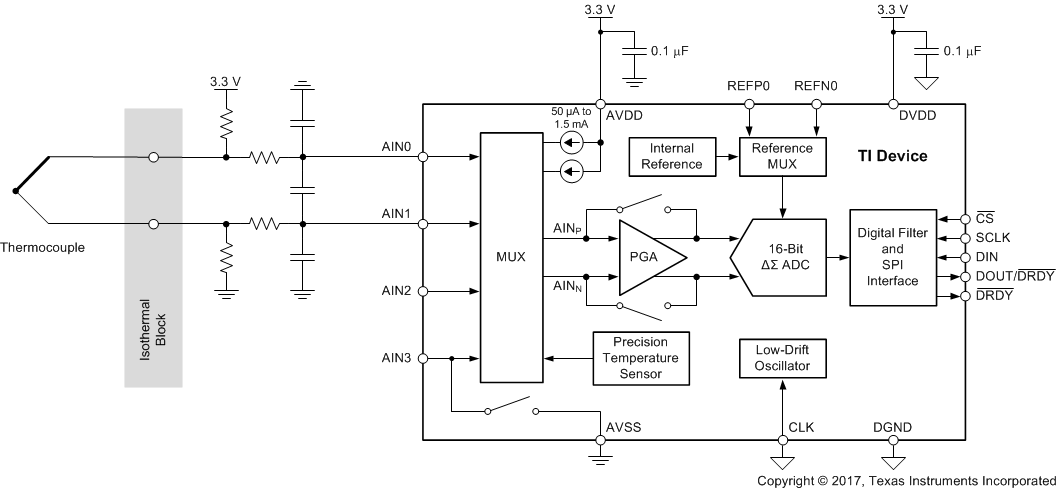
The ADS1120 is a precision, 16-bit, analog-to-digital converter (ADC) that offers many integrated features to reduce system cost and component count in applications measuring small sensor signals. The device features two differential or four single-ended inputs through a flexible input multiplexer (MUX), a low-noise, programmable gain amplifier (PGA), two programmable excitation current sources, a voltage reference, an oscillator, a low-side switch, and a precision temperature sensor.
The device can perform conversions at data rates up to 2000 samples-per-second (SPS) with single-cycle settling. At 20 SPS, the digital filter offers simultaneous 50-Hz and 60-Hz rejection for noisy industrial applications. The internal PGA offers gains up to 128 V/V. This PGA makes the ADS1120 ideally-suited for applications measuring small sensor signals, such as resistance temperature detectors (RTDs), thermocouples, thermistors, and bridge sensors. The device supports measurements of pseudo- or fully-differential signals when using the PGA. Alternatively, the device can be configured to bypass the internal PGA while still providing high input impedance and gains up to 4 V/V, allowing for single-ended measurements.
Power consumption is as low as 120 µA when operating in duty-cycle mode with the PGA disabled. The ADS1120 is offered in a leadless VQFN-16 or a TSSOP-16 package and is specified over a temperature range of –40°C to +125°C.
Device Information(1)
| PART NUMBER | PACKAGE | BODY SIZE (NOM) |
|---|---|---|
| ADS1120 | VQFN (16) | 3.50 mm × 3.50 mm |
| TSSOP (16) | 5.00 mm × 4.40 mm |
- For all available packages, see the orderable addendum at the end of the datasheet.
4 Revision History
Changes from B Revision (January 2015) to C Revision
- Changed document title Go
- Changed K-Type Thermocouple Measurement figure Go
- Added footnote 1 to Pin Functions table and changed descriptions of AIN0/REFP1, AIN1, AIN2, AIN3/REFN1, REFN0, and REFP0 pins accordingly Go
- Changed format of Absolute Maximum Ratings tableGo
- Changed Functional Block Diagram figure Go
- Changed Bypassing the PGA sectionGo
- Changed (AVDD) to (AVDD – AVSS) in first paragraph of Voltage Reference sectionGo
- Added fourth sentence to Temperature Sensor sectionGo
- Changed last equation in Converting from Digital Codes to Temperature sectionGo
- Changed bit 0 in register 03h to 0 from RESERVED Go
- Changed description of bits 5:4 in Configuration Register 2Go
- Added Unused Inputs and Outputs section Go
- Changed Thermocouple Measurement figureGo
- Changed 3-Wire RTD Measurement figure Go
- Changed 2-Wire RTD Measurement figure Go
- Changed 4-Wire RTD Measurement figure Go
- Changed Resistive Bridge Measurement figure Go
- Changed Power Supply Recommendations section: changed Power-Supply Sequencing subsection, added Power-Supply Ramp Rate subsectionGo
Changes from A Revision (January 2014) to B Revision
- Added ESD Ratings and Recommended Operating Conditions tables and Application and Implementation, Power Supply Recommendations, Layout, Device and Documentation Support, and Mechanical, Packaging, and Orderable Information sectionsGo
- Changed document title, Features, Applications, Description, Pin Configuration and Functions, Parameter Measurement Information, Feature Description, Device Functional Modes, Programming, and Register Map sections, and front-page figureGo
- Deleted Ordering Information section and Product Family tableGo
- Changed format of Absolute Maximum Ratings table and added minimum junction temperature specificationGo
- Changed Analog Inputs and Voltage Reference Input sections (specification values were not changed) and added Internal Oscillator section to Electrical Characteristics tableGo
- Changed System Performance section: changed VIO parameter name, deleted symbol and changed test conditions of Gain error parameter in Electrical Characteristics table Go
- Deleted Clock Sources section and changed Temperature Sensor and Power Supply sections (specification values were not changed) in Electrical Characteristics tableGo
- Changed SPI Timing Requirements and Figure 1 (specification values were not changed), added SPI Switching Characteristics and Figure 2 Go
- Changed format of Typical Characteristics section (actual curves did not change)Go
Changes from * Revision (August 2013) to A Revision
- Released to productionGo
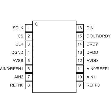
5 Pin Configuration and Functions


Pin Functions
| PIN | ANALOG OR DIGITAL INPUT/OUTPUT |
DESCRIPTION(1) | ||
|---|---|---|---|---|
| NAME | NO. | |||
| RVA | PW | |||
| AIN0/REFP1 | 9 | 11 | Analog input | Analog input 0, positive reference input 1 |
| AIN1 | 8 | 10 | Analog input | Analog input 1 |
| AIN2 | 5 | 7 | Analog input | Analog input 2 |
| AIN3/REFN1 | 4 | 6 | Analog input | Analog input 3, negative reference input 1. Internal low-side power switch connected between AIN3/REFN1 and AVSS. |
| AVDD | 10 | 12 | Analog | Positive analog power supply |
| AVSS | 3 | 5 | Analog | Negative analog power supply |
| CLK | 1 | 3 | Digital input | External clock source pin. Connect to DGND if not used. |
| CS | 16 | 2 | Digital input | Chip select; active low. Connect to DGND if not used. |
| DGND | 2 | 4 | Digital | Digital ground |
| DIN | 14 | 16 | Digital input | Serial data input |
| DOUT/DRDY | 13 | 15 | Digital output | Serial data output combined with data ready; active low |
| DRDY | 12 | 14 | Digital output | Data ready, active low. Leave unconnected or tie to DVDD using a weak pull-up resistor if not used. |
| DVDD | 11 | 13 | Digital | Positive digital power supply |
| REFN0 | 6 | 8 | Analog input | Negative reference input 0 |
| REFP0 | 7 | 9 | Analog input | Positive reference input 0 |
| SCLK | 15 | 1 | Digital input | Serial clock input |
| Thermal pad | — | — | Thermal power pad. Do not connect or only connect to AVSS. | |
