SBAS607B April 2016 – September 2016 ADS127L01
PRODUCTION DATA.
- 1 Features
- 2 Applications
- 3 Description
- 4 Revision History
- 5 Pin Configuration and Functions
-
6 Specifications
- 6.1 Absolute Maximum Ratings
- 6.2 ESD Ratings
- 6.3 Recommended Operating Conditions
- 6.4 Thermal Information
- 6.5 Electrical Characteristics
- 6.6 Timing Requirements: Serial Interface
- 6.7 Switching Characteristics: Serial Interface Mode
- 6.8 Timing Requirements: Frame-Sync Master Mode
- 6.9 Switching Characteristics: Frame-Sync Master Mode
- 6.10 Timing Requirements: Frame-Sync Slave Mode
- 6.11 Switching Characteristics: Frame-Sync Slave Mode
- 6.12 Typical Characteristics
- 7 Parameter Measurement information
-
8 Detailed Description
- 8.1 Overview
- 8.2 Functional Block Diagram
- 8.3 Feature Description
- 8.4 Device Functional Modes
- 8.5
Programming
- 8.5.1 Serial Peripheral Interface (SPI) Programming
- 8.5.2
Frame-Sync Programming
- 8.5.2.1
Frame-Sync Master Mode
- 8.5.2.1.1 Chip Select (CS) in Frame-Sync Master Mode
- 8.5.2.1.2 Serial Clock (SCLK) in Frame-Sync Master Mode
- 8.5.2.1.3 Frame-Sync (DRDY/FSYNC) in Frame-Sync Master Mode
- 8.5.2.1.4 Data Input (DIN) in Frame-Sync Master Mode
- 8.5.2.1.5 Data Output (DOUT) in Frame-Sync Master Mode
- 8.5.2.1.6 Daisy-Chain Input (DAISYIN) in Frame-Sync Master Mode
- 8.5.2.2
Frame-Sync Slave Mode
- 8.5.2.2.1 Chip Select (CS) in Frame-Sync Slave Mode
- 8.5.2.2.2 Serial Clock (SCLK) in Frame-Sync Slave Mode
- 8.5.2.2.3 Frame-Sync (DRDY/FSYNC) in Frame-Sync Slave Mode
- 8.5.2.2.4 Data Input (DIN) in Frame-Sync Slave Mode
- 8.5.2.2.5 Data Output (DOUT) in Frame-Sync Slave Mode
- 8.5.2.2.6 Daisy-Chain Input (DAISYIN) in Frame-Sync Slave Mode
- 8.5.2.1
Frame-Sync Master Mode
- 8.5.3 Data Format
- 8.5.4 Status Word
- 8.5.5 Cyclic Redundancy Check (CRC)
- 8.6
Register Maps
- 8.6.1 ID: ID Control Register (address = 00h) [reset = x3h]
- 8.6.2 CONFIG: ADC Configuration Register (address = 01h) [reset = 00h]
- 8.6.3 OFC0: System Offset Calibration Register 0 (address = 02h) [reset = 00h]
- 8.6.4 OFC1: System Offset Calibration Register 1 (address = 03h) [reset = 00h]
- 8.6.5 OFC2: System Offset Calibration Register 2 (address = 04h) [reset = 00h]
- 8.6.6 FSC0: System Gain Calibration Register 0 (address = 05h) [reset = 00h]
- 8.6.7 FSC1: System Gain Calibration Register 1 (address = 06h) [reset = 80h]
- 8.6.8 MODE: Mode Settings (address = 07h) [reset = xxh]
- 9 Application and Implementation
- 10Power Supply Recommendations
- 11Layout
- 12Device and Documentation Support
- 13Mechanical, Packaging, and Orderable Information
Package Options
Mechanical Data (Package|Pins)
- PBS|32
Thermal pad, mechanical data (Package|Pins)
- PBS|32
Orderable Information
1 Features
- Data Rates: Up to 512 kSPS
- AC + DC Performance:
- Operating Modes:
- Digital Filter Options:
- Low-latency Filter: Sinc Frequency Response
- Wideband 1 Filter:
(0.45 to 0.55) × fDATA Transition Band - Wideband 2 Filter:
(0.40 to 0.50) × fDATA Transition Band
- SPI™ or Frame-Sync Serial Interface
- Daisy-Chain Compatible
- Analog Supply: 2.7 V to 3.6 V
- Digital Supply: 1.7 V to 3.6 V
- Operating Temperature: –40°C to +125°C
2 Applications
- Vibration and Modal Analysis
- Data Acquisition Systems
- Acoustics and Dynamic Strain Gauges
- Power Quality Analysis
3 Description
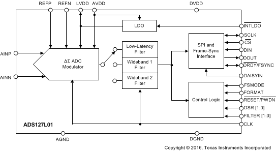
The ADS127L01 is a 24-bit, delta-sigma (ΔΣ), analog-to-digital converter (ADC) with data rates up to 512 kSPS. This device offers a unique combination of excellent dc accuracy and outstanding ac performance. The high-order, chopper-stabilized modulator achieves very low drift with low in-band noise. The integrated decimation filter suppresses modulator out-of-band noise. In addition to al low-latency filter, the ADS127L01 provides multiple Wideband filters with less than ±0.00004 dB of ripple, and an option for –116-dB stop-band attenuation at the Nyquist rate.
Traditionally, industrial delta-sigma ADCs that offer good drift performance use digital filters with large passband droop. As a result, industrial delta-sigma ADCs have limited signal bandwidth and are mostly suited for dc measurements. High-resolution ADCs in audio applications offer larger usable bandwidths, but the offset and drift specifications are significantly weaker than industrial counterparts. The ADS127L01 combines these converters, providing high-precision industrial measurement with excellent dc and ac specifications over an extended industrial temperature range of –40°C to +125°C.
A variety of operating modes allow for optimization of speed, resolution, and power. A programmable serial interface with one of three options (SPI, frame-sync slave, or frame-sync master) provides convenient interfacing across isolation barriers to microcontrollers or digital signal processors (DSPs).
Device Information(1)
| PART NUMBER | PACKAGE | BODY SIZE (NOM) |
|---|---|---|
| ADS127L01 | TQFP (32) | 5.00 mm × 5.00 mm |
- For all available packages, see the package option addendum at the end of the data sheet.
ADS127L01 Block Diagram

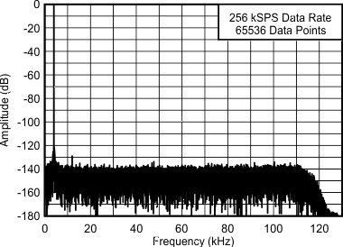
ADC Frequency Spectrum
