-
ADS1283 High-Resolution, Analog-to-Digital Converter
- 1 Features
- 2 Applications
- 3 Description
- 4 Revision History
- 5 Pin Configuration and Functions
- 6 Specifications
- 7 Parameter Measurement Information
-
8 Detailed Description
- 8.1 Overview
- 8.2 Functional Block Diagram
- 8.3 Feature Description
- 8.4
Device Functional Modes
- 8.4.1 Synchronization (SYNC PIN and SYNC Command)
- 8.4.2 Reset (RESET Pin and Reset Command)
- 8.4.3 Power-Down (PWDN Pin and STANDBY Command)
- 8.4.4 Power-On Sequence
- 8.4.5 DVDD Power Supply
- 8.4.6 Serial Interface
- 8.4.7 Data Format
- 8.4.8 Reading Data
- 8.4.9 One-Shot Operation
- 8.4.10 Offset and Full-Scale Calibration Registers
- 8.4.11 Calibration Commands (OFSCAL and GANCAL)
- 8.4.12 User Calibration
- 8.5
Programming
- 8.5.1
Commands
- 8.5.1.1 SDATAC Requirements
- 8.5.1.2 WAKEUP: Wake-Up From Standby Mode
- 8.5.1.3 STANDBY: Standby Mode
- 8.5.1.4 SYNC: Synchronize the Analog-to-Digital Conversion
- 8.5.1.5 RESET: Reset the Device
- 8.5.1.6 RDATAC: Read Data Continuous
- 8.5.1.7 SDATAC: Stop Read Data Continuous
- 8.5.1.8 RDATA: Read Data by Command
- 8.5.1.9 RREG: Read Register Data
- 8.5.1.10 WREG: Write to Register
- 8.5.1.11 OFSCAL: Offset Calibration
- 8.5.1.12 GANCAL: Gain Calibration
- 8.5.1
Commands
- 8.6
Register Maps
- 8.6.1
Register Descriptions
- 8.6.1.1 ID_CFG: ID_Configuration Register (address = 00h) [reset =x0h]
- 8.6.1.2 CONFIG0: Configuration Register 0 (address = 01h) [reset = 52h]
- 8.6.1.3 CONFIG1: Configuration Register 1 (address = 02h) [reset = 08h]
- 8.6.1.4 HPF0 and HPF1 Registers
- 8.6.1.5 OFC0, OFC1, OFC2 Registers
- 8.6.1.6 FSC0, FSC1, FSC2 Registers
- 8.6.1
Register Descriptions
- 9 Application and Implementation
- 10Device and Documentation Support
- 11Mechanical, Packaging, and Orderable Information
- IMPORTANT NOTICE
Package Options
Mechanical Data (Package|Pins)
- RHF|24
Thermal pad, mechanical data (Package|Pins)
Orderable Information
ADS1283 High-Resolution, Analog-to-Digital Converter
1 Features
- High Resolution:
- SNR: 130 dB (250 SPS, PGA = 1)
- High Accuracy:
- THD: –122 dB
- Low Power Consumption:
- 18 mW (PGA = 1, 2, 4, or 8)
- Shutdown Mode: 10 μW
- Low-Noise PGA: 5 nV/√Hz
- Two-Channel Input Multiplexer
- Inherently-Stable Modulator With Fast Responding Overrange Detector
- Flexible Digital Filter:
- Sinc + FIR + IIR (Selectable)
- Linear or Minimum Phase Response
- Programmable High-Pass Filter
- Selectable FIR Data Rates:
250 SPS to 4 kSPS
- Offset and Gain Calibration Engine
- SYNC Input
- Analog Supply: 5 V or ±2.5 V
- Digital Supply: 1.8 V to 3.3 V
2 Applications
- Energy Exploration
- Seismic Monitoring
- High-Accuracy Instrumentation
Simplified Schematic

3 Description
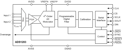
The ADS1283 is an extremely high-performance, single-chip, analog-to-digital converter (ADC) with an integrated, low-noise programmable gain amplifier (PGA) and two-channel input multiplexer (mux). The ADS1283 is suitable for the demanding needs of seismic monitoring equipment.
The converter uses a fourth-order, inherently stable, delta-sigma (ΔΣ) modulator that provides outstanding noise and linearity performance. The modulator digital output is digitally filtered and decimated by the on-chip digital filter to yield the ADC conversion result.
The flexible input mux provides an additional external input for measurement, as well as internal self-test input connections. The PGA features outstanding low noise (5 nV/√Hz) and very-high input impedance, allowing easy interfacing to geophones and hydrophones over a wide range of gains.
The digital filter provides selectable data rates from 250 to 4000 samples per second (SPS). The high-pass filter (HPF) features an adjustable corner frequency. On-chip gain and offset scaling registers support system calibration.
The synchronization input (SYNC) can be used to synchronize the conversions of multiple ADS1283 devices.
The ADS1283 is available in a compact 24-lead, 5-mm × 4-mm VQFN package, and is fully specified from –40°C to +85°C, with a maximum operating temperature range of –50°C to +125°C.
Device Information(1)
| PART NUMBER | PACKAGE | BODY SIZE (NOM) |
|---|---|---|
| ADS1283 | VQFN (24) | 5.00 mm × 4.00 mm |
| ADS1283A | ||
| ADS1283B |
- For all available packages, see the package option addendum at the end of the data sheet.
Device Comparison
| PART NUMBER | OFFSET OPTION | THD (TYP) | GAIN |
|---|---|---|---|
| ADS1283 | 100 mV | –122 dB | 1 to 64 |
| ADS1283A | 100 mV | –118 dB | 1, 4, 16 |
| ADS1283B | 75 mV, 100 mV | –122 dB | 1 to 64 |