-
ADS41xx 14-, 12-Bit, 65-, 125-MSPS, Ultra-Low-Power ADC
- 1 Features
- 2 Applications
- 3 Description
- 4 Revision History
- 5 Device Family Comparison
- 6 Pin Configuration and Functions
-
7 Specifications
- 7.1 Absolute Maximum Ratings
- 7.2 ESD Ratings
- 7.3 Recommended Operating Conditions
- 7.4 Thermal Information
- 7.5 Electrical Characteristics: ADS412x
- 7.6 Electrical Characteristics: ADS414x
- 7.7 Electrical Characteristics: General
- 7.8 Digital Characteristics
- 7.9 Timing Requirements: LVDS and CMOS Modes
- 7.10 Serial Interface Timing Characteristics
- 7.11 Reset Timing Requirements
- 7.12 Timing Characteristics at Lower Sampling Frequencies
- 7.13 Typical Characteristics: ADS4122
- 7.14 Typical Characteristics: ADS4125
- 7.15 Typical Characteristics: ADS4142
- 7.16 Typical Characteristics: ADS4145
- 7.17 Typical Characteristics: Common
- 7.18 Typical Characteristics: Contour
- 8 Detailed Description
- 9 Application and Implementation
- 10Power Supply Recommendations
- 11Layout
- 12Device and Documentation Support
- 13Mechanical, Packaging, and Orderable Information
- IMPORTANT NOTICE
Package Options
Mechanical Data (Package|Pins)
- RGZ|48
Thermal pad, mechanical data (Package|Pins)
- RGZ|48
Orderable Information
ADS41xx 14-, 12-Bit, 65-, 125-MSPS, Ultra-Low-Power ADC
1 Features
- Ultra-Low Power With 1.8-V Single Supply:
- 103-mW Total Power at 65 MSPS
- 153-mW Total Power at 125 MSPS
- High Dynamic Performance:
- SNR: 72.2 dBFS at 170 MHz
- SFDR: 81 dBc at 170 MHz
- Dynamic Power Scaling With Sample Rate
- Idle Channel SNR 74.8 dBFS (ADS414x)
- Output Interface:
- Double Data Rate (DDR) LVDS With Programmable Swing and Strength:
- Standard Swing: 350 mV
- Low Swing: 200 mV
- Default Strength: 100-Ω Termination
- 2x Strength: 50-Ω Termination
- 1.8-V Parallel CMOS Interface Also Supported
- Double Data Rate (DDR) LVDS With Programmable Swing and Strength:
- Programmable Gain up to 6 dB for SNR, SFDR Trade-Off
- DC Offset Correction
- Supports Low Input Clock Amplitude Down to 200 mVPP
2 Applications
3 Description
The ADS412x and ADS414x devices are lower-sampling speed variants in the ADS41xx family of analog-to-digital converters (ADCs). These devices use innovative design techniques to achieve high dynamic performance, while consuming extremely low power at 1.8-V supply. The devices are well-suited for multi-carrier, wide bandwidth communications applications.
The ADS412x and ADS414x devices have fine gain options that can be used to improve SFDR performance at lower full-scale input ranges, especially at high input frequencies. They include a dc offset correction loop that can be used to cancel the ADC offset. At lower sampling rates, the ADC automatically operates at scaled down power with no loss in performance.
The ADS412x and ADS414x devices are available in a compact VQFN-48 package and are specified over the industrial temperature range (–40°C to +85°C).
Device Information(1)
| PART NUMBER | PACKAGE | BODY SIZE (NOM) |
|---|---|---|
| ADS4122 | VQFN (48) | 7.00 mm × 7.00 mm |
| ADS4125 | ||
| ADS4142 | ||
| ADS4145 |
- For all available packages, see the orderable addendum at the end of the data sheet.
4 Revision History
Changes from B Revision (January 2016) to C Revision
- Added a new feature Idle Channel SNR 74.8 dBFS (ADS414x) to the Features sectionGo
- Added a new application Imaging Systems in Applications sectionGo
- Changed ADS412x/4x to ADS412x and ADS414x in Description sectionGo
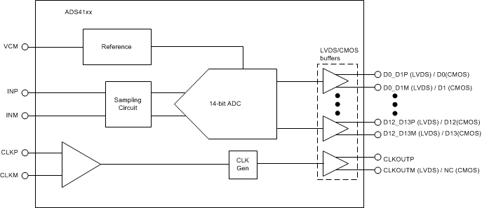
- Changed ADS41xx Block Diagram in the first page.Go
- Changed input clock sample rate minimum for the ADS4122/ADS4142, low-speed mode enabled by default from: 20 MSPS to: 3 MSPS Go
- Changed input clock sample rate minimum for the ADS4122/ADS4142, low-speed mode enabled from: 20 MSPS to: 3 MSPS Go
- Deleted High Performance Modes section from Recommended Operating Conditions table, moved to Programming sectionGo
- Added order to HD2 and HD3 parameter names in Electrical Characteristics tablesGo
- Added test conditions header to Electrical Characteristics: General table Go
- Added Using the ADS41xx at Low Sampling Rates subsection in Application and Implementation sectionGo
- Added Figure 114 to Figure 124 in ADS412x (12-Bit Device) sectionGo
- Changed the order of figures in ADS412x (12-Bit Device) section. Go
- Added the device name ADS412x to the conditions of ADS412x (12-Bit Device) section.Go
- Changed the unit of fS from MHz to MSPS in the specifications of Figure 115Go
- Added new subsection ADS412x (12-Bit Device) in Application Information section. Go
- Changed the unit of fS from MHz to MSPS in the specifications of Figure 116Go
- Changed the unit of fS from MHz to MSPS in the specifications of Figure 119 Go
- Changed the unit of fS from MHz to MSPS in the specifications of Figure 120 Go
- Changed the unit of fS from MHz to MSPS in the specifications of Figure 121 Go
- Changed the unit of fS from MHz to MSPS in the specifications of Figure 122 Go
- Added Figure 125 through Figure 128 in typical performance at lower sampling rate for ADS412x (12-bit devices) in CMOS interface mode. Go
- Added Figure 129 through Figure 130 in typical performance at lower sampling rate for ADS412x (12-bit devices) in CMOS interface mode. Go
- Added Figure 131 through Figure 132 in typical performance at lower sampling rate for ADS412x (12-bit devices) in CMOS interface mode. Go
- Added Figure 136 to Figure 146 in ADS414x (14-Bit Device) sectionGo
- Changed the order of figures in ADS414x (14-Bit Device) section.Go
- Added the device name ADS414x to the conditions of ADS414x (14-Bit Device) section. Go
- Changed the unit of fS from MHz to MSPS in the specifications of Figure 137 and Figure 138Go
- Added new subsection ADS414x (14-Bit Device) in Application Information section.Go
- Changed the SNR and SINAD values of Figure 138 .Go
- Changed the unit of fS from MHz to MSPS in the specifications of Figure 141 through Figure 144Go
- Added Figure 147 through Figure 157 in typical performance at lower sampling rate for ADS414x (14-bit devices) in CMOS interface mode. Go
- Added Figure 151 through Figure 158 in typical performance at lower sampling rate for ADS414x (14-bit devices) in CMOS interface mode. Go
- Added Figure 153 through Figure 155 in typical performance at lower sampling rate for ADS414x (14-bit devices) in CMOS interface mode. Go
- Added Output Timing at Low Sampling Rates subsection in Application and Implementation sectionGo
- Changed the name of the header from ADS4128 CAPABILITY to ADS4125 CAPABILITY in the last column of Table 10 Go
- Added Receiving Notification of Documentation Updates section Go
Changes from A Revision (March 2011) to B Revision
- Added Pin Configuration and Functions section, Handling Rating table, Feature Descriptionsection, Device Functional Modes, Application and Implementation section, Power Supply Recommendations section, Layout section, Device and Documentation Supportsection, and Mechanical, Packaging, and Orderable Information section Go
6 Pin Configuration and Functions


NOINDENT:
The thermal pad is connected to DRGND.Pin Functions: LVDS Mode
| PIN | I/O | DESCRIPTION | ||
|---|---|---|---|---|
| NAME | ADS412x | ADS414x | ||
| AGND | 9, 12, 14, 17, 19, 25 | 9, 12, 14, 17, 19, 25 | I | Analog ground |
| AVDD | 8, 18, 20, 22, 24, 26 | 8, 18, 20, 22, 24, 26 | I | 1.8-V analog power supply |
| CLKM | 11 | 11 | I | Differential clock input, complement |
| CLKP | 10 | 10 | I | Differential clock input, true |
| CLKOUTM | 4 | 4 | O | Differential output clock, complement |
| CLKOUTP | 5 | 5 | O | Differential output clock, true |
| D0_D1_M | 37 | 33 | O | Differential output data D0 and D1 multiplexed, complement |
| D0_D1_P | 38 | 34 | O | Differential output data D0 and D1 multiplexed, true |
| D2_D3_M | 39 | 37 | O | Differential output data D2 and D3 multiplexed, complement |
| D2_D3_P | 40 | 38 | O | Differential output data D2 and D3 multiplexed, true |
| D4_D5_M | 41 | 39 | O | Differential output data D4 and D5 multiplexed, complement |
| D4_D5_P | 42 | 40 | O | Differential output data D4 and D5 multiplexed, true |
| D6_D7_M | 43 | 41 | O | Differential output data D6 and D7 multiplexed, complement |
| D6_D7_P | 44 | 42 | O | Differential output data D6 and D7 multiplexed, true |
| D8_D9_M | 45 | 43 | O | Differential output data D8 and D9 multiplexed, complement |
| D8_D9_P | 46 | 44 | O | Differential output data D8 and D9 multiplexed, true |
| D10_D11_M | 47 | 45 | O | Differential output data D10 and D11 multiplexed, complement |
| D10_D11_P | 48 | 46 | O | Differential output data D10 and D11 multiplexed, true |
| D12_D13_M | — | 47 | O | Differential output data D12 and D13 multiplexed, complement |
| D12_D13_P | — | 48 | O | Differential output data D12 and D13 multiplexed, true |
| DFS | 6 | 6 | I | Data format select input. This pin sets the DATA FORMAT (twos complement or offset binary) and the LVDS, CMOS output interface type. See Table 5 for detailed information. |
| DRGND | 1, 36, PAD | 1, 36, PAD | I | Digital and output buffer ground |
| DRVDD | 2, 35 | 2, 35 | I | 1.8-V digital and output buffer supply |
| INM | 16 | 16 | I | Differential analog input, negative |
| INP | 15 | 15 | I | Differential analog input, positive |
| NC | 21, 31, 32, 33, 34 | 21, 31, 32 | – | Do not connect |
| OE | 7 | 7 | I | Output buffer enable input, active high; this pin has an internal 180-kΩ pullup resistor to DRVDD. |
| OVR_SDOUT | 3 | 3 | O | This pin functions as an out-of-range indicator after reset, when register bit READOUT = 0, and functions as a serial register readout pin when READOUT = 1. |
| RESERVED | 23 | 23 | I | Digital control pin, reserved for future use |
| RESET | 30 | 30 | I | Serial interface RESET input. When using the serial interface mode, the internal registers must initialize through hardware RESET by applying a high pulse on this pin or by using the software reset option; see the Serial Interface section. When RESET is tied high, the internal registers are reset to the default values. In this condition, SEN can be used as an analog control pin. RESET has an internal 180-kΩ pulldown resistor. |
| SCLK | 29 | 29 | I | This pin functions as a serial interface clock input when RESET is low. When RESET is high, SCLK has no function and should be tied to ground. This pin has an internal 180-kΩ pulldown resistor. |
| SDATA | 28 | 28 | I | This pin functions as a serial interface data input when RESET is low. When RESET is high, SDATA functions as a STANDBY control pin (see Table 7). This pin has an internal 180-kΩ pulldown resistor. |
| SEN | 27 | 27 | I | This pin functions as a serial interface enable input when RESET is low. When RESET is high, SEN has no function and must be tied to AVDD. This pin has an internal 180-kΩ pullup resistor to AVDD. |
| VCM | 13 | 13 | O | Outputs the common-mode voltage (0.95 V) that can be used externally to bias the analog input pins. |


Pin Functions: CMOS Mode
| PIN | I/O | DESCRIPTION | ||
|---|---|---|---|---|
| NAME | ADS412x | ADS414x | ||
| AVDD | 8, 18, 20, 22, 24, 26 | 8, 18, 20, 22, 24, 26 | I | 1.8-V analog power supply |
| AGND | 9, 12, 14, 17, 19, 25 | 9, 12, 14, 17, 19, 25 | I | Analog ground |
| CLKM | 11 | 11 | I | Differential clock input, complement |
| CLKP | 10 | 10 | I | Differential clock input, true |
| CLKOUT | 5 | 5 | O | CMOS output clock |
| D0 | 37 | 33 | O | 12-bit, 14-bit CMOS output data |
| D1 | 38 | 34 | O | 12-bit, 14-bit CMOS output data |
| D2 | 39 | 37 | O | 12-bit, 14-bit CMOS output data |
| D3 | 40 | 38 | O | 12-bit, 14-bit CMOS output data |
| D4 | 41 | 39 | O | 12-bit, 14-bit CMOS output data |
| D5 | 42 | 40 | O | 12-bit, 14-bit CMOS output data |
| D6 | 43 | 41 | O | 12-bit, 14-bit CMOS output data |
| D7 | 44 | 42 | O | 12-bit, 14-bit CMOS output data |
| D8 | 45 | 43 | O | 12-bit, 14-bit CMOS output data |
| D9 | 46 | 44 | O | 12-bit, 14-bit CMOS output data |
| D10 | 47 | 45 | O | 12-bit, 14-bit CMOS output data |
| D11 | 48 | 46 | O | 12-bit, 14-bit CMOS output data |
| D12 | — | 47 | O | 12-bit, 14-bit CMOS output data |
| D13 | — | 48 | O | 12-bit, 14-bit CMOS output data |
| DFS | 6 | 6 | I | Data format select input. This pin sets the DATA FORMAT (twos complement or offset binary) and the LVDS, CMOS output interface type. See Table 5 for detailed information. |
| DRGND | 1, 36, PAD | 1, 36, PAD | I | Digital and output buffer ground |
| DRVDD | 2, 35 | 2, 35 | I | 1.8-V digital and output buffer supply |
| INM | 16 | 16 | I | Differential analog input, negative |
| INP | 15 | 15 | I | Differential analog input, positive |
| NC | 21, 31, 32, 33, 34 | 21, 31, 32 | – | Do not connect |
| OE | 7 | 7 | I | Output buffer enable input, active high; this pin has an internal 180-kΩ pullup resistor to DRVDD. |
| OVR_SDOUT | 3 | 3 | O | This pin functions as an out-of-range indicator after reset, when register bit READOUT = 0, and functions as a serial register readout pin when READOUT = 1. |
| RESERVED | 23 | 23 | I | Digital control pin, reserved for future use |
| RESET | 30 | 30 | I | Serial interface RESET input. When using the serial interface mode, the internal registers must initialize through hardware RESET by applying a high pulse on this pin or by using the software reset option; see the Serial Interface section. When RESET is tied high, the internal registers are reset to the default values. In this condition, SEN can be used as an analog control pin. RESET has an internal 180-kΩ pulldown resistor. |
| SCLK | 29 | 29 | I | This pin functions as a serial interface clock input when RESET is low. When RESET is high, SCLK has no function and must be tied to ground. This pin has an internal 180-kΩ pulldown resistor. |
| SDATA | 28 | 28 | I | This pin functions as a serial interface data input when RESET is low. When RESET is high, SDATA functions as a STANDBY control pin (see Table 7). This pin has an internal 180-kΩ pulldown resistor. |
| SEN | 27 | 27 | I | This pin functions as a serial interface enable input when RESET is low. When RESET is high, SEN has no function and must be tied to AVDD. This pin has an internal 180-kΩ pullup resistor to AVDD. |
| UNUSED | 4 | 4 | – | Unused pin in CMOS mode |
| VCM | 13 | 13 | O | Outputs the common-mode voltage (0.95 V) that can be used externally to bias the analog input pins. |
7 Specifications
7.1 Absolute Maximum Ratings
Over operating free-air temperature range, unless otherwise noted.(1)| MIN | MAX | UNIT | ||
|---|---|---|---|---|
| Supply voltage, AVDD | –0.3 | 2.1 | V | |
| Supply voltage, DRVDD | –0.3 | 2.1 | V | |
| Voltage between AGND and DRGND | –0.3 | 0.3 | V | |
| Voltage between AVDD to DRVDD (when AVDD leads DRVDD) | 0 | 2.1 | V | |
| Voltage between DRVDD to AVDD (when DRVDD leads AVDD) | 0 | 2.1 | V | |
| Voltage applied to input pins | INP, INM | –0.3 | minimum (1.9, AVDD + 0.3) | V |
| CLKP, CLKM(2), DFS, OE | –0.3 | AVDD + 0.3 | ||
| RESET, SCLK, SDATA, SEN | –0.3 | 3.9 | ||
| Operating free-air temperature, TA | –40 | 85 | °C | |
| Operating junction temperature, TJ | 125 | °C | ||
| Storage temperature, Tstg | –65 | 150 | °C | |
7.2 ESD Ratings
| VALUE | UNIT | |||
|---|---|---|---|---|
| V(ESD) | Electrostatic discharge | Human-body model (HBM), per ANSI/ESDA/JEDEC JS-001(1) | ±2000 | V |
| Charged-device model (CDM), per JEDEC specification JESD22-C101(2) | ±500 | |||
7.3 Recommended Operating Conditions
Over operating free-air temperature range, unless otherwise noted.| MIN | NOM | MAX | UNIT | |||
|---|---|---|---|---|---|---|
| SUPPLIES | ||||||
| AVDD | Analog supply voltage | 1.7 | 1.8 | 1.9 | V | |
| DRVDD | Digital supply voltage | 1.7 | 1.8 | 1.9 | V | |
| ANALOG INPUTS | ||||||
| Differential input voltage(1) | 2 | VPP | ||||
| Input common-mode voltage | VCM ± 0.05 | V | ||||
| Maximum analog input frequency with 2-VPP input amplitude(2) | 400 | MHz | ||||
| Maximum analog input frequency with 1-VPP input amplitude(2) | 800 | MHz | ||||
| CLOCK INPUT | ||||||
| Input clock sample rate | ADS4122, ADS4142, low-speed mode enabled by default | 3 | 65 | MSPS | ||
| ADS4125, ADS4145, low-speed mode enabled | 3 | 80 | ||||
| ADS4125, ADS4145, low-speed mode disabled | > 80 | 125 | ||||
| Input clock amplitude differential (VCLKP – VCLKM) |
Sine wave, ac-coupled | 0.2 | 1.5 | VPP | ||
| LVPECL, ac-coupled | 1.6 | |||||
| LVDS, ac-coupled | 0.7 | |||||
| LVCMOS, single-ended, ac-coupled | 1.8 | V | ||||
| Input clock duty cycle | Low-speed enabled | 40% | 50% | 60% | ||
| Low-speed disabled | 35% | 50% | 65% | |||
| DIGITAL OUTPUTS | ||||||
| CLOAD | Maximum external load capacitance from each output pin to DRGND | 5 | pF | |||
| RLOAD | Differential load resistance between the LVDS output pairs (LVDS mode) | 100 | Ω | |||
| TA | Operating free-air temperature | –40 | 85 | °C | ||
7.4 Thermal Information
| THERMAL METRIC(1) | ADS412x, ADS414x |
UNIT | |
|---|---|---|---|
| RGZ (VQFN) | |||
| 48 PIN | |||
| RθJA | Junction-to-ambient thermal resistance | 29 | °C/W |
| RθJCtop | Junction-to-case (top) thermal resistance | N/A | °C/W |
| RθJB | Junction-to-board thermal resistance | 10 | °C/W |
| ψJT | Junction-to-top characterization parameter | 0.3 | °C/W |
| ψJB | Junction-to-board characterization parameter | 9 | °C/W |
| RθJCbot | Junction-to-case (bottom) thermal resistance | 1.1 | °C/W |
7.5 Electrical Characteristics: ADS412x
Typical values are at 25°C, AVDD = 1.8 V, DRVDD = 1.8 V, 50% clock duty cycle, –1-dBFS differential analog input, 0-dB gain, and DDR LVDS interface, unless otherwise noted. Minimum and maximum values are across the full temperature range: TMIN = –40°C to TMAX = 85°C, AVDD = 1.8 V, and DRVDD = 1.8 V.7.6 Electrical Characteristics: ADS414x
Typical values are at 25°C, AVDD = 1.8 V, DRVDD = 1.8 V, 50% clock duty cycle, –1-dBFS differential analog input, 0-dB gain, and DDR LVDS interface, unless otherwise noted. Minimum and maximum values are across the full temperature range: TMIN = –40°C to TMAX = 85°C, AVDD = 1.8 V, and DRVDD = 1.8 V.| PARAMETER | TEST CONDITIONS | MIN | TYP | MAX | UNIT | ||
|---|---|---|---|---|---|---|---|
| Resolution | 14 | Bits | |||||
| SNR | Signal-to-noise ratio, LVDS | fIN = 10 MHz | ADS4142 (65 MSPS) | 73.9 | dBFS | ||
| ADS4145 (125 MSPS) | 73.7 | ||||||
| fIN = 70 MHz | ADS4142 (65 MSPS) | 73.5 | |||||
| ADS4145 (125 MSPS) | 73.4 | ||||||
| fIN = 100 MHz | ADS4142 (65 MSPS) | 73.2 | |||||
| ADS4145 (125 MSPS) | 73.1 | ||||||
| fIN = 170 MHz | ADS4142 (65 MSPS) | 69 | 72.4 | ||||
| ADS4145 (125 MSPS) | 70 | 72.2 | |||||
| fIN = 300 MHz | ADS4142 (65 MSPS) | 70.5 | |||||
| ADS4145 (125 MSPS) | 71.3 | ||||||
| SINAD | Signal-to-noise and distortion ratio, LVDS | fIN = 10 MHz | ADS4142 (65 MSPS) | 73.5 | dBFS | ||
| ADS4145 (125 MSPS) | 73.2 | ||||||
| fIN = 70 MHz | ADS4142 (65 MSPS) | 73.3 | |||||
| ADS4145 (125 MSPS) | 73 | ||||||
| fIN = 100 MHz | ADS4142 (65 MSPS) | 73 | |||||
| ADS4145 (125 MSPS) | 72.6 | ||||||
| fIN = 170 MHz | ADS4142 (65 MSPS) | 68 | 72.3 | ||||
| ADS4145 (125 MSPS) | 69 | 71.8 | |||||
| fIN = 300 MHz | ADS4142 (65 MSPS) | 69.2 | |||||
| ADS4145 (125 MSPS) | 70.6 | ||||||
| SFDR | Spurious-free dynamic range | fIN = 10 MHz | ADS4142 (65 MSPS) | 87 | dBc | ||
| ADS4145 (125 MSPS) | 86 | ||||||
| fIN = 70 MHz | ADS4142 (65 MSPS) | 86.5 | |||||
| ADS4145 (125 MSPS) | 85.5 | ||||||
| fIN = 100 MHz | ADS4142 (65 MSPS) | 87 | |||||
| ADS4145 (125 MSPS) | 82 | ||||||
| fIN = 170 MHz | ADS4142 (65 MSPS) | 71 | 85 | ||||
| ADS4145 (125 MSPS) | 72.5 | 81.5 | |||||
| fIN = 300 MHz | ADS4142 (65 MSPS) | 72.5 | |||||
| ADS4145 (125 MSPS) | 77 | ||||||
| THD | Total harmonic distortion | fIN = 10 MHz | ADS4142 (65 MSPS) | 84 | dBc | ||
| ADS4145 (125 MSPS) | 83 | ||||||
| fIN = 70 MHz | ADS4142 (65 MSPS) | 84 | |||||
| ADS4145 (125 MSPS) | 83.5 | ||||||
| fIN = 100 MHz | ADS4142 (65 MSPS) | 84 | |||||
| ADS4145 (125 MSPS) | 81 | ||||||
| fIN = 170 MHz | ADS4142 (65 MSPS) | 69.5 | 82.5 | ||||
| ADS4145 (125 MSPS) | 70.5 | 80 | |||||
| fIN = 300 MHz | ADS4142 (65 MSPS) | 72.5 | |||||
| ADS4145 (125 MSPS) | 75.5 | ||||||
| HD2 | Second-order harmonic distortion | fIN = 10 MHz | ADS4142 (65 MSPS) | 88 | dBc | ||
| ADS4145 (125 MSPS) | 87 | ||||||
| fIN = 70 MHz | ADS4142 (65 MSPS) | 87 | |||||
| ADS4145 (125 MSPS) | 85.5 | ||||||
| fIN = 100 MHz | ADS4142 (65 MSPS) | 88 | |||||
| ADS4145 (125 MSPS) | 82 | ||||||
| fIN = 170 MHz | ADS4142 (65 MSPS) | 71 | 87 | ||||
| ADS4145 (125 MSPS) | 72.5 | 84 | |||||
| fIN = 300 MHz | ADS4142 (65 MSPS) | 72.5 | |||||
| ADS4145 (125 MSPS) | 77 | ||||||
| HD3 | Third-order harmonic distortion | fIN = 10 MHz | ADS4142 (65 MSPS) | 87 | dBc | ||
| ADS4145 (125 MSPS) | 86 | ||||||
| fIN = 70 MHz | ADS4142 (65 MSPS) | 86.5 | |||||
| ADS4145 (125 MSPS) | 87 | ||||||
| fIN = 100 MHz | ADS4142 (65 MSPS) | 87 | |||||
| ADS4145 (125 MSPS) | 85 | ||||||
| fIN = 170 MHz | ADS4142 (65 MSPS) | 71 | 85 | ||||
| ADS4145 (125 MSPS) | 72.5 | 81.5 | |||||
| fIN = 300 MHz | ADS4142 (65 MSPS) | 85 | |||||
| ADS4145 (125 MSPS) | 84 | ||||||
| Worst spur (other than second and third harmonics) |
fIN = 10 MHz | ADS4142 (65 MSPS) | 96 | dBc | |||
| ADS4145 (125 MSPS) | 95 | ||||||
| fIN = 70 MHz | 95 | ||||||
| fIN = 100 MHz | ADS4142 (65 MSPS) | 94 | |||||
| ADS4145 (125 MSPS) | 95 | ||||||
| fIN = 170 MHz | ADS4142 (65 MSPS) | 77.5 | 92 | ||||
| ADS4145 (125 MSPS) | 78.5 | 91 | |||||
| fIN = 300 MHz | ADS4142 (65 MSPS) | 87 | |||||
| ADS4145 (125 MSPS) | 88 | ||||||
| IMD | Two-tone intermodulation distortion | f1 = 100 MHz, f2 = 105 MHz, each tone at –7 dBFS |
ADS4142 (65 MSPS) | 88.5 | dBFS | ||
| ADS4145 (125 MSPS) | 87.5 | ||||||
| Input overload recovery | Recovery to within 1% (of final value) for 6-dB overload with sine-wave input | 1 | Clock cycles | ||||
| PSRR | AC power-supply rejection ratio | For 100-mVPP signal on AVDD supply, up to 10 MHz | > 30 | dB | |||
| ENOB | Effective number of bits | fIN = 170 MHz | ADS4142 (65 MSPS) | 11.5 | LSBs | ||
| ADS4145 (125 MSPS) | 11.3 | ||||||
| DNL | Differential nonlinearity | fIN = 170 MHz | –0.95 | ±0.5 | 1.7 | LSBs | |
| INL | Integrated nonlinearity | fIN = 170 MHz | ±1.5 | ±4.5 | LSBs | ||
7.7 Electrical Characteristics: General
Typical values are at 25°C, AVDD = 1.8 V, DRVDD = 1.8 V, 50% clock duty cycle, and 0-dB gain, unless otherwise noted. Minimum and maximum values are across the full temperature range: TMIN = –40°C to TMAX = 85°C, AVDD = 1.8 V, and DRVDD = 1.8 V.| PARAMETER | TEST CONDITIONS | MIN | TYP | MAX | UNIT | |
|---|---|---|---|---|---|---|
| ANALOG INPUTS | ||||||
| Differential input voltage | 2 | VPP | ||||
| Differential input resistance | At dc, see Figure 106 | > 1 | MΩ | |||
| Differential input capacitance | See Figure 107 | 4 | pF | |||
| Analog input bandwidth | 550 | MHz | ||||
| Analog input common-mode current (per input pin) | 0.6 | µA/MSPS | ||||
| VCM | Common-mode output voltage | 0.95 | V | |||
| VCM output current capability | 4 | mA | ||||
| DC ACCURACY | ||||||
| Offset error | –15 | 2.5 | 15 | mV | ||
| Temperature coefficient of offset error | 0.003 | mV/°C | ||||
| EGREF | Gain error as a result of internal reference inaccuracy alone | –2 | 2 | %FS | ||
| EGCHAN | Gain error of channel alone | –0.2 | %FS | |||
| Temperature coefficient of EGCHAN | 0.001 | Δ%/°C | ||||
| POWER SUPPLY | ||||||
| IAVDD | Analog supply current | ADS4122, ADS4142 (65 MSPS) | 42 | 55 | mA | |
| ADS4125, ADS4145 (125 MSPS) | 62 | 75 | ||||
| IDRVDD(2) | Output buffer supply current, LVDS interface with 100-Ω external termination, low LVDS swing (200 mV) | ADS4122, ADS4142 (65 MSPS) | 28.5 | mA | ||
| ADS4125, ADS4145 (125 MSPS) | 35.5 | |||||
| Output buffer supply current, LVDS interface with 100-Ω external termination, standard LVDS swing (350 mV) | ADS4122, ADS4142 (65 MSPS) | 40 | 53 | |||
| ADS4125, ADS4145 (125 MSPS) | 48 | 57 | ||||
| Output buffer supply current(2)(1), CMOS interface(1), 8-pF external load capacitance, fIN = 2.5 MHz |
ADS4122, ADS4142 (65 MSPS) | 15 | ||||
| ADS4125, ADS4145 (125 MSPS) | 23 | |||||
| Analog power | ADS4122, ADS4142 (65 MSPS) | 76 | mW | |||
| ADS4122, ADS4142 (125 MSPS) | 112 | |||||
| Digital power, LVDS interface, low LVDS swing | ADS4122, ADS4142 (65 MSPS) | 52 | mW | |||
| ADS4122, ADS4142 (125 MSPS) | 66.5 | |||||
| Digital power, CMOS interface(1), 8-pF external load capacitance, fIN = 2.5 MHz | ADS4122, ADS4142 (65 MSPS) | 27 | mW | |||
| ADS4122, ADS4142 (125 MSPS) | 41.5 | |||||
| Global power-down | 10 | 15 | mW | |||
| Standby | ADS4122, ADS4142 (65 MSPS) | 105 | mW | |||
| ADS4122, ADS4142 (125 MSPS) | 130 | |||||
7.8 Digital Characteristics
Typical values are at 25°C, AVDD = 1.8 V, DRVDD = 1.8 V, and 50% clock duty cycle for the ADS4122, ADS4125, ADS4142, and ADS4145, unless otherwise noted. Minimum and maximum values are across the full temperature range: TMIN = –40°C to TMAX = 85°C, AVDD = 1.8 V, and DRVDD = 1.8 V.| PARAMETER | TEST CONDITIONS | MIN | TYP | MAX | UNIT | |
|---|---|---|---|---|---|---|
| DIGITAL INPUTS (RESET, SCLK, SDATA, SEN, OE) | ||||||
| High-level input voltage | RESET, SCLK, SDATA, and SEN support 1.8-V and 3.3-V CMOS logic levels | 1.3 | V | |||
| Low-level input voltage | 0.4 | V | ||||
| High-level input voltage | OE only supports 1.8-V CMOS logic levels | 1.3 | V | |||
| Low-level input voltage | 0.4 | V | ||||
| High-level input current: SDATA, SCLK(1) | VHIGH = 1.8 V | 10 | µA | |||
| High-level input current: SEN | VHIGH = 1.8 V | 0 | µA | |||
| Low-level input current: SDATA, SCLK | VLOW = 0 V | 0 | µA | |||
| Low-level input current: SEN | VLOW = 0 V | –10 | µA | |||
| DIGITAL OUTPUTS (CMOS INTERFACE: D0 TO D13, OVR_SDOUT) | ||||||
| High-level output voltage | DRVDD – 0.1 | DRVDD | V | |||
| Low-level output voltage | 0 | 0.1 | V | |||
| DIGITAL OUTPUTS (LVDS INTERFACE: DA0P/M TO DA13P/M, DB0P/M TO DB13P/M, CLKOUTP/M) | ||||||
| High-level output voltage(2) | VODH | Standard swing LVDS | 270 | 350 | 430 | mV |
| Low-level output voltage(2) | VODL | Standard swing LVDS | –430 | –350 | –270 | mV |
| High-level output voltage(2) | VODH | Low swing LVDS | 200 | mV | ||
| Low-level output voltage(2) | VODL | Low swing LVDS | –200 | mV | ||
| Output common-mode voltage | VOCM | 0.85 | 1.05 | 1.25 | V | |
7.9 Timing Requirements: LVDS and CMOS Modes(1)
Typical values are at 25°C, AVDD = 1.8 V, DRVDD = 1.8 V, sampling frequency = 125 MSPS, sine wave input clock, CLOAD = 5 pF(2), and RLOAD = 100 Ω(3), unless otherwise noted. Minimum and maximum values are across the full temperature range: TMIN = –40°C to TMAX = 85°C, AVDD = 1.8 V, and DRVDD = 1.7 V to 1.9 V.| MIN | TYP | MAX | UNIT | |||
|---|---|---|---|---|---|---|
| GENERAL | ||||||
| tA | Aperture delay | 0.6 | 0.8 | 1.2 | ns | |
| Variation of aperture delay between two devices at the same temperature and DRVDD supply | ±100 | ps | ||||
| tJ | Aperture jitter | 100 | fS rms | |||
| Wakeup time: | Time to valid data after coming out of STANDBY mode | 5 | 25 | µs | ||
| Time to valid data after coming out of PDN GLOBAL mode | 100 | 500 | µs | |||
| ADC latency(4): | Low-latency mode (default after reset) | 10 | Clock cycles | |||
| Low-latency mode disabled (gain enabled, offset correction disabled) | 16 | Clock cycles | ||||
| Low-latency mode disabled (gain and offset correction enabled) | 17 | Clock cycles | ||||
| DDR LVDS MODE(5)(6) | ||||||
| tSU | Data setup time(3): data valid(7) to zero-crossing of CLKOUTP | 2.3 | 3 | ns | ||
| tH | Data hold time(3): zero-crossing of CLKOUTP to data becoming invalid(7) | 0.35 | 0.6 | ns | ||
| tPDI | Clock propagation delay: input clock rising edge cross-over to output clock rising edge cross-over, sampling frequency ≤ 125 MSPS | 3 | 4.2 | 5.4 | ns | |
| Variation of tPDI between two devices at the same temperature and DRVDD supply | ±0.6 | ns | ||||
| LVDS bit clock duty cycle of differential clock, (CLKOUTP – CLKOUTM), sampling frequency ≤ 125 MSPS | 48% | |||||
| tRISE, tFALL | Data rise time, data fall time: rise time measured from –100 mV to 100 mV, fall time measured from 100 mV to –100 mV, sampling frequency ≤ 125 MSPS | 0.14 | ns | |||
| tCLKRISE, tCLKFALL | Output clock rise time, output clock fall time rise time measured from –100 mV to 100 mV, fall time measured from 100 mV to –100 mV, sampling frequency ≤ 125 MSPS | 0.14 | ns | |||
| tOE | Output enable (OE) to data delay: time to valid data after OE becomes active | 50 | 100 | ns | ||
| PARALLEL CMOS MODE(8) | ||||||
| tSETUP | Data setup time: data valid(9) to 50% of CLKOUT rising edge | 3.1 | 3.7 | ns | ||
| tHOLD | Data hold time: 50% of of CLKOUT rising edge to data becoming invalid(9) | 3.2 | 4 | ns | ||
| tPDI | Clock propagation delay: input clock rising edge cross-over to 50% of output clock rising edge, sampling frequency ≤ 125 MSPS | 4 | 5.5 | 7 | ns | |
| Output clock duty cycle of output clock, CLKOUT, sampling frequency ≤ 125 MSPS | 47% | |||||
| tRISE, tFALL | Data rise time, data fall time: rise time measured from 20% to 80% of DRVDD, fall time measured from 80% to 20% of DRVDD, sampling frequency ≤ 125 MSPS | 0.35 | ns | |||
| tCLKRISE, tCLKFALL | Output clock rise time, output clock fall time: rise time measured from 20% to 80% of DRVDD, fall time measured from 80% to 20% of DRVDD, sampling frequency ≤ 125 MSPS | 0.35 | ns | |||
| tOE | Output enable (OE) to data delay: time to valid data after OE becomes active | 20 | 40 | ns | ||
7.10 Serial Interface Timing Characteristics
Typical values at 25°C, minimum and maximum values across the full temperature range: TMIN = –40°C to TMAX = 85°C, AVDD = 1.8 V, and DRVDD = 1.8 V, unless otherwise noted.| PARAMETER | MIN | TYP | MAX | UNIT | |
|---|---|---|---|---|---|
| fSCLK | SCLK frequency (equal to 1/tSCLK) | > dc | 20 | MHz | |
| tSLOADS | SEN to SCLK setup time | 25 | ns | ||
| tSLOADH | SCLK to SEN hold time | 25 | ns | ||
| tDSU | SDATA setup time | 25 | ns | ||
| tDH | SDATA hold time | 25 | ns | ||
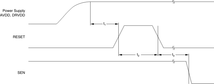
7.11 Reset Timing Requirements
Typical values at 25°C and minimum and maximum values across the full temperature range: TMIN = –40°C to TMAX = 85°C, unless otherwise noted.| MIN | TYP | MAX | UNIT | |||
|---|---|---|---|---|---|---|
| t1 | Power-on delay from power-up of AVDD and DRVDD to RESET pulse active | 1 | ms | |||
| t2 | Reset pulse duration of active RESET signal that resets the serial registers | 10 | ns | |||
| 1(1) | µs | |||||
| t3 | Delay from RESET disable to SEN active | 100 | ns | |||
7.12 Timing Characteristics at Lower Sampling Frequencies
| SAMPLING FREQUENCY (MSPS) | tsu, SETUP TIME | th, HOLD TIME | tPDI, CLOCK PROPAGATION DELAY | UNIT | ||||||
|---|---|---|---|---|---|---|---|---|---|---|
| MIN | TYP | MAX | MIN | TYP | MAX | MIN | TYP | MAX | ||
| DDR LVDS | ns | |||||||||
| 65 | 5.5 | 6.5 | 0.35 | 0.6 | ns | |||||
| 80 | 4.5 | 5.2 | 0.35 | 0.6 | ns | |||||
| CMOS (LOW LATENCY ENABLED)(1) | ns | |||||||||
| 65 | 6.5 | 7.5 | 6.5 | 7.5 | 4 | 5.5 | 7 | ns | ||
| 80 | 5.4 | 6 | 5.4 | 6 | 4 | 5.5 | 7 | ns | ||
| CMOS (LOW LATENCY DISABLED)(1) | ns | |||||||||
| 65 | 6 | 7 | 7 | 8 | 4 | 5.5 | 7 | ns | ||
| 80 | 4.8 | 5.5 | 5.7 | 6.5 | 4 | 5.5 | 7 | ns | ||
| 125 | 2.5 | 3.2 | 3.5 | 4.3 | 4 | 5.5 | 7 | ns | ||

NOINDENT:
With external 100-Ω termination.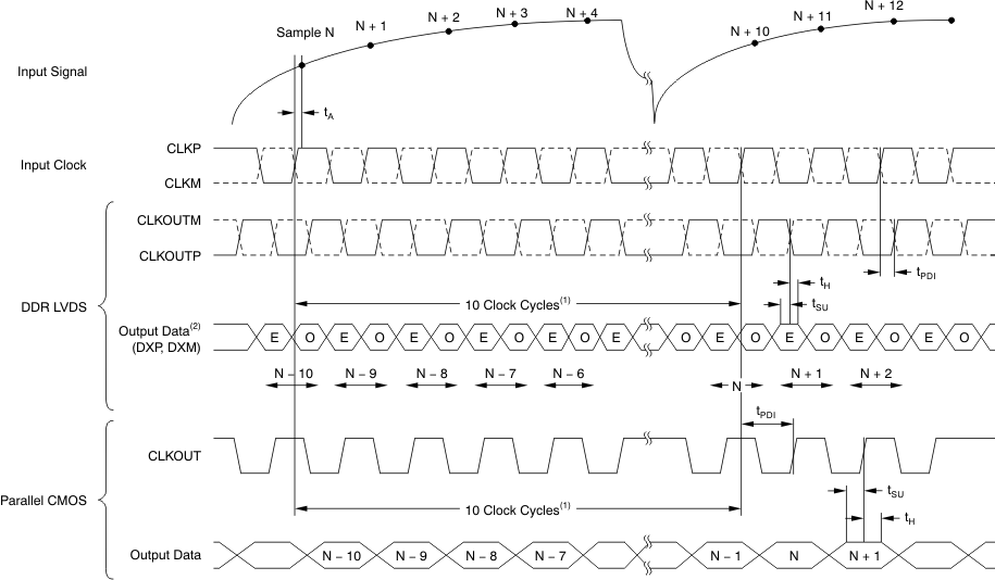
NOINDENT:
ADC latency in low-latency mode. At higher sampling frequencies, tDPI is greater than one clock cycle which then makes the overall latency = ADC latency + 1.NOINDENT:
E = Even bits (D0, D2, D4, and so forth). O = Odd bits (D1, D3, D5, and so forth).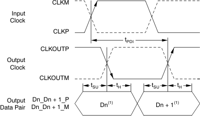
NOINDENT:
Dn = bits D0, D2, D4, and so forth. Dn + 1 = Bits D1, D3, D5, and so forth.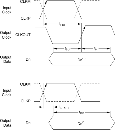
NOINDENT:
Dn = bits D0, D1, D2, and so forth. Figure 5. Serial Interface Timing
NOINDENT:
A high pulse on the RESET pin is required in the serial interface mode in case of initialization through hardware reset. For parallel interface operation, RESET must be permanently tied high.7.13 Typical Characteristics: ADS4122
At 25°C, AVDD = 1.8 V, DRVDD = 1.8 V, maximum-rated sampling frequency, sine wave input clock, 1.5-VPP differential clock amplitude, 50% clock duty cycle, –1-dBFS differential analog input, 0-dB gain, low-latency mode, DDR LVDS output interface, and 32k-point FFT, unless otherwise noted.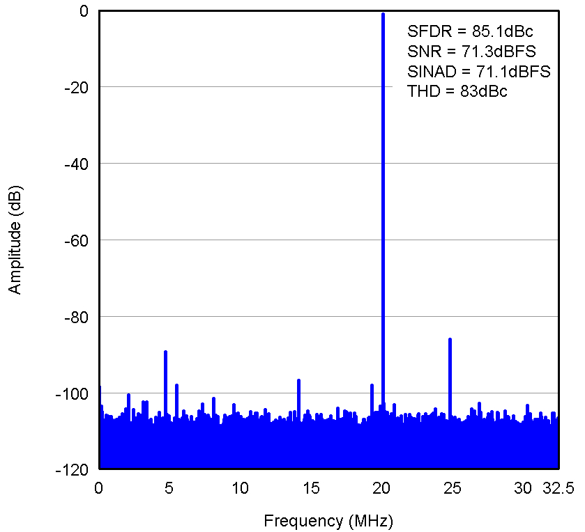 Figure 7. FFT for 20-MHz Input Signal
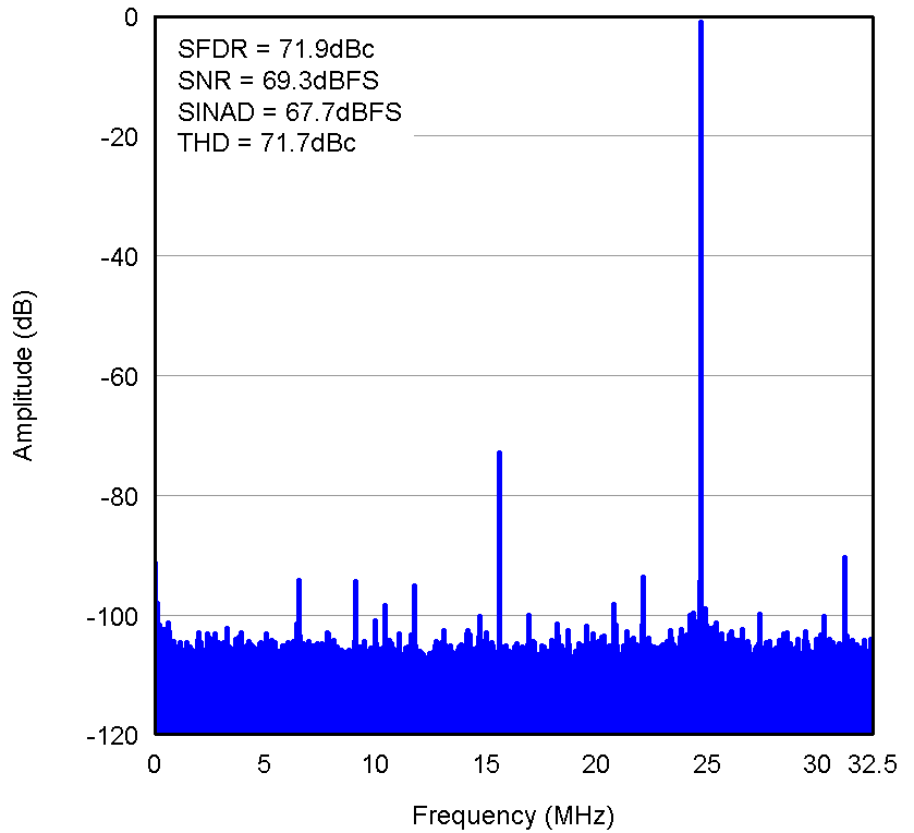 Figure 9. FFT for 300-MHz Input Signal
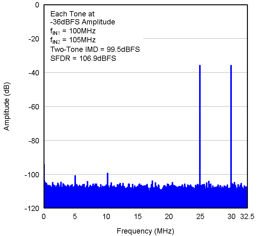 Figure 11. FFT for Two-Tone Input Signal
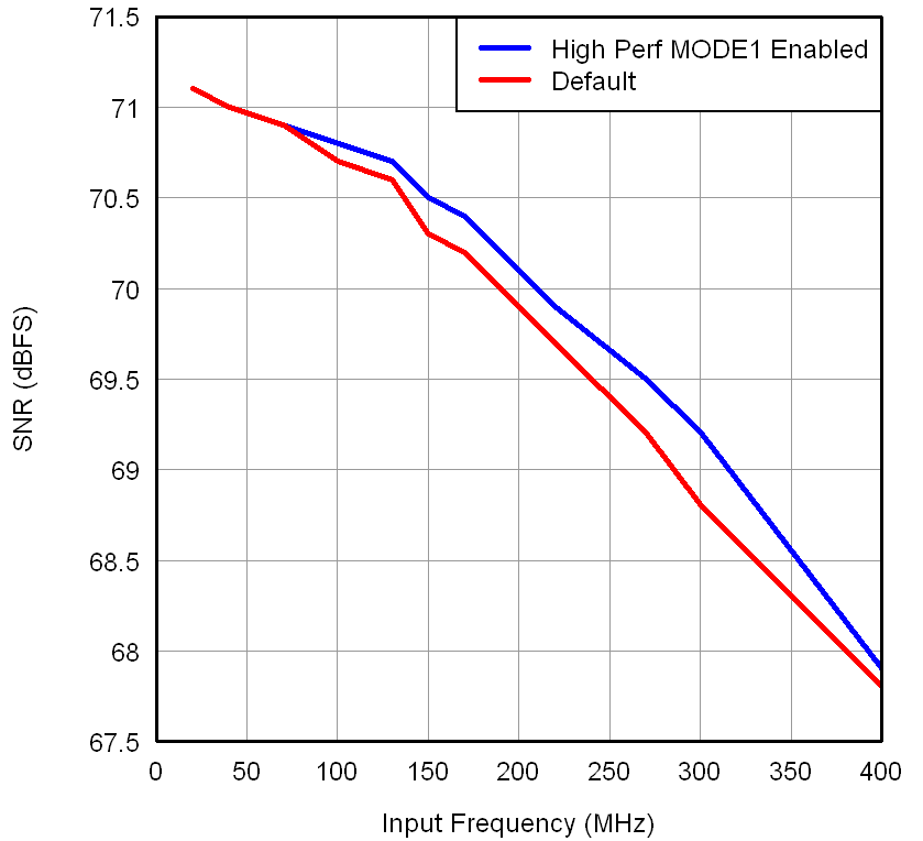 Figure 13. SNR vs Input Frequency
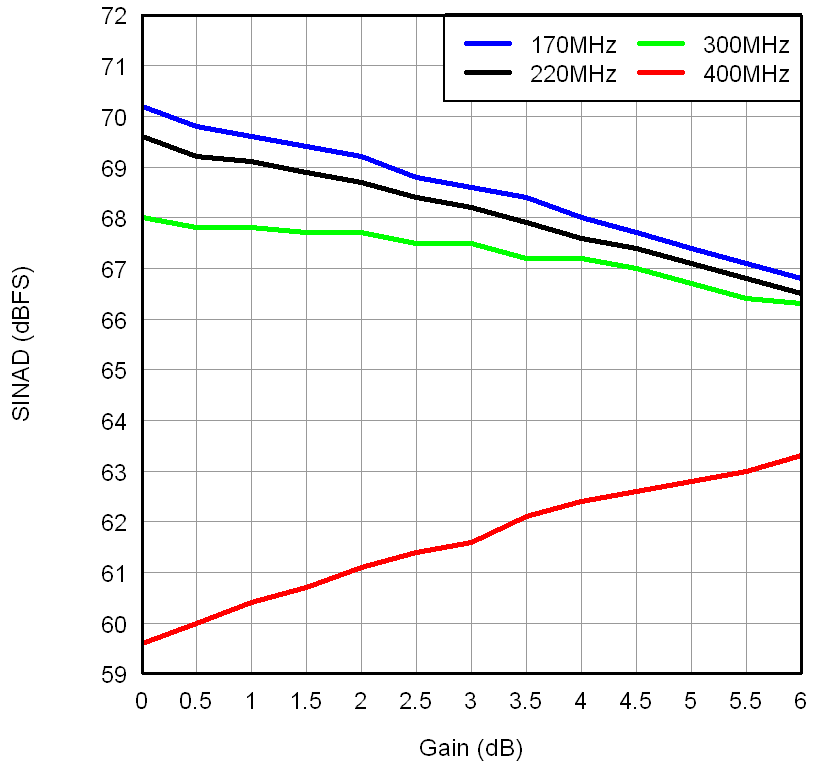 Figure 15. SINAD Across Gain and Input Frequency
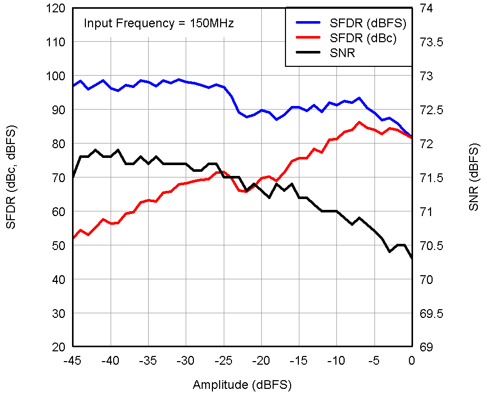 Figure 17. Performance Across Input Amplitude
(Single Tone)
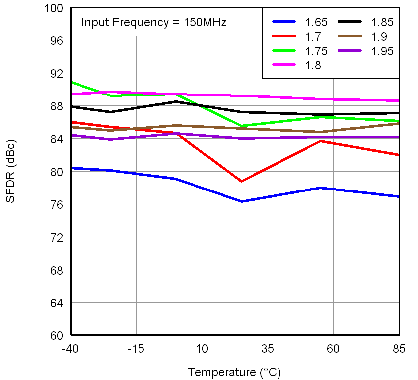 Figure 19. SFDR Across Temperature vs AVDD Supply
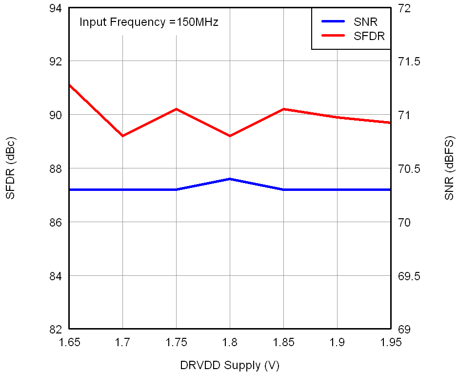 Figure 21. Performance Across DRVDD Supply Voltage
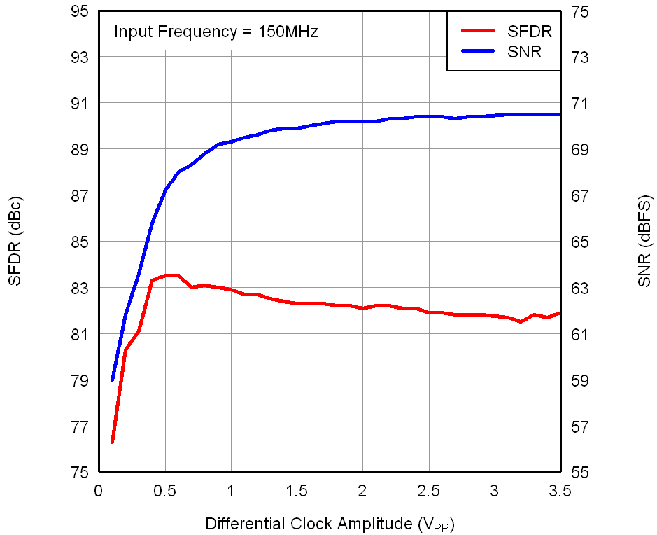 Figure 23. Performance Across Input Clock Amplitude
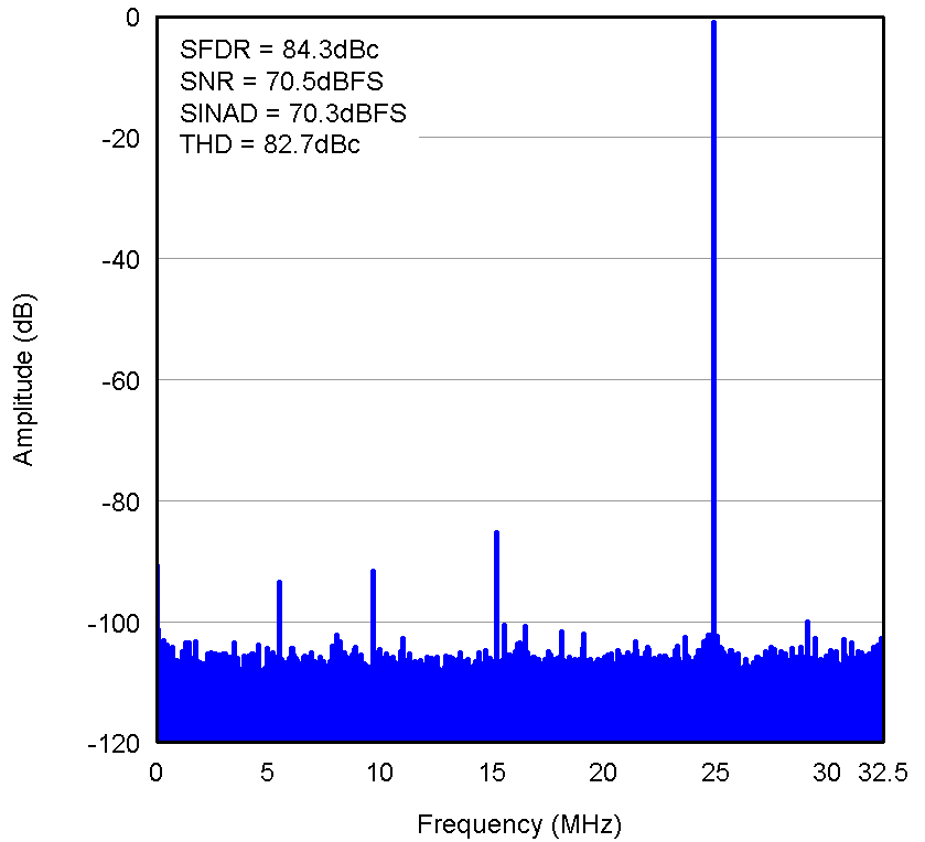 Figure 8. FFT for 170-MHz Input Signal
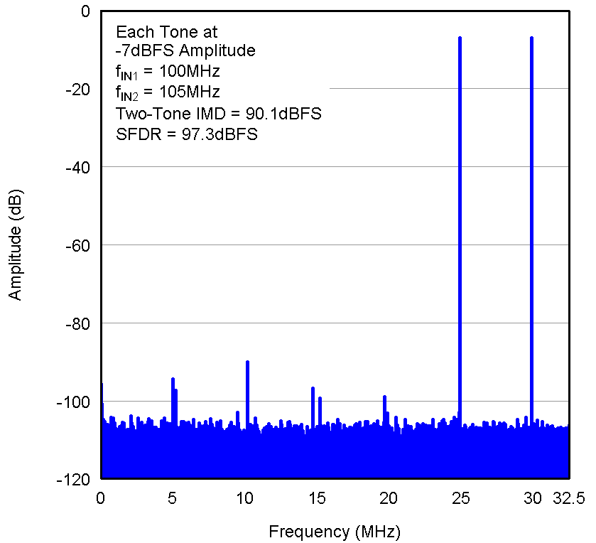 Figure 10. FFT for Two-Tone Input Signal
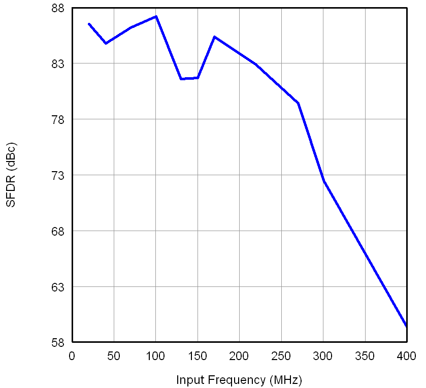 Figure 12. SFDR vs Input Frequency
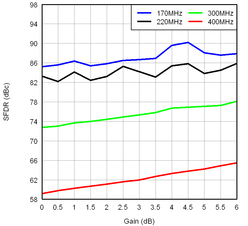 Figure 14. SFDR Across Gain and Input Frequency
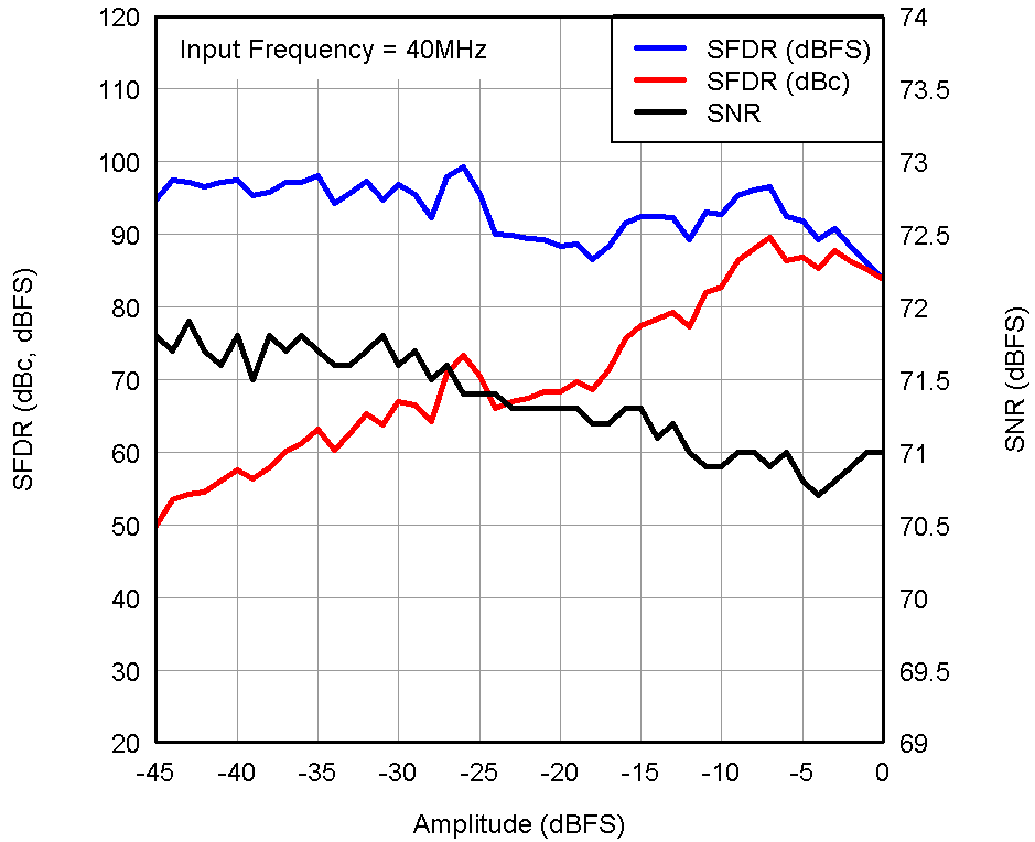 Figure 16. Performance Across Input Amplitude
 (Single Tone)
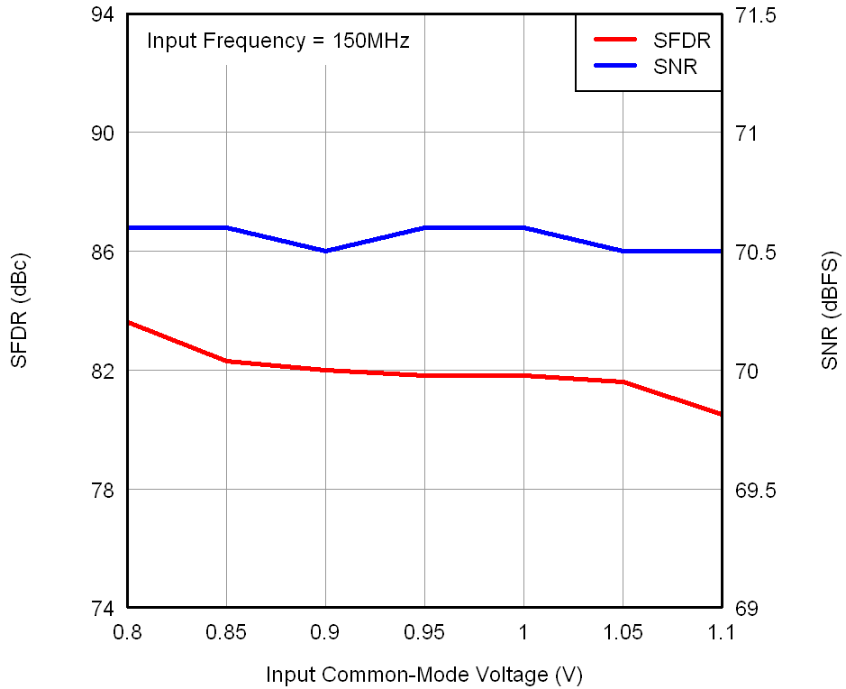 Figure 18. Performance vs Input Common-Mode Voltage
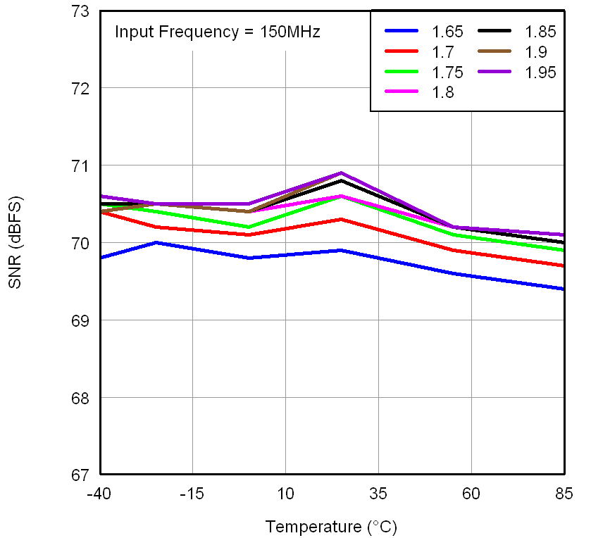 Figure 20. SNR Across Temperature vs AVDD Supply
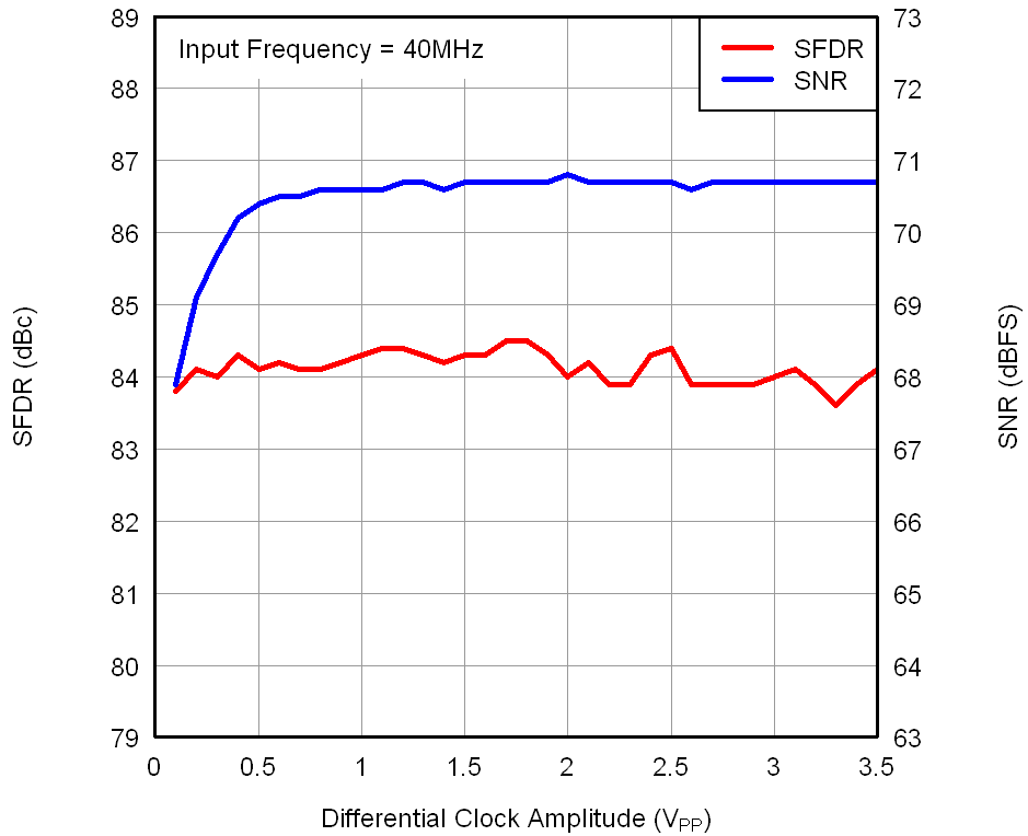 Figure 22. Performance Across Input Clock Amplitude
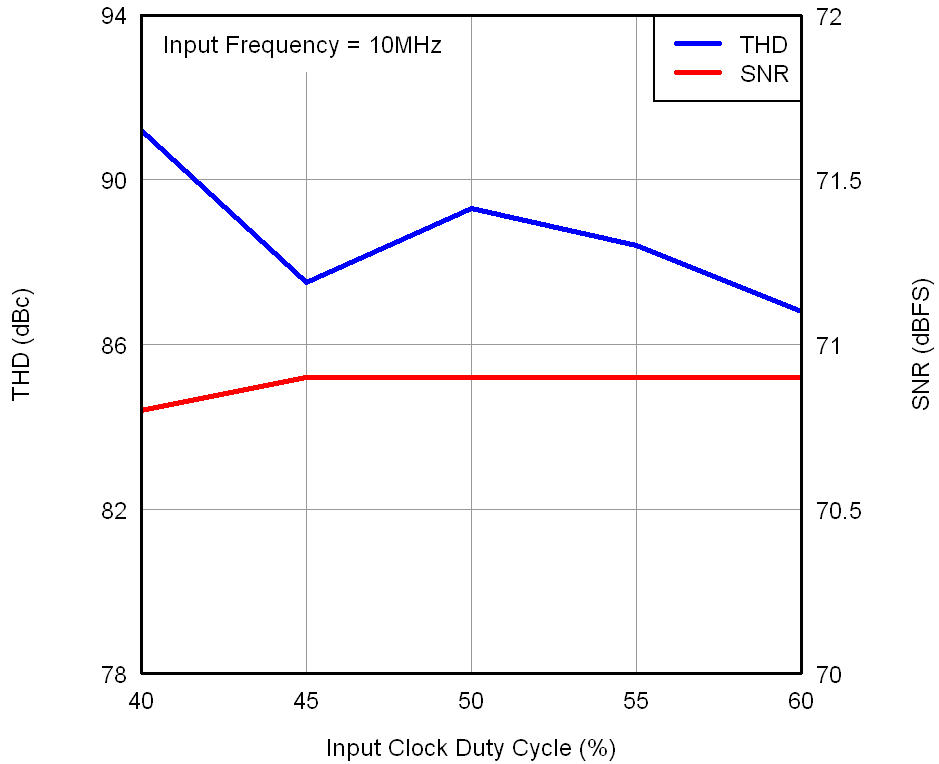 Figure 24. Performance Across Input Clock Duty Cycle
7.14 Typical Characteristics: ADS4125
At 25°C, AVDD = 1.8 V, DRVDD = 1.8 V, maximum-rated sampling frequency, sine wave input clock, 1.5-VPP differential clock amplitude, 50% clock duty cycle, –1-dBFS differential analog input, 0-dB gain, low-latency mode, DDR LVDS output interface, and 32k-point FFT, unless otherwise noted.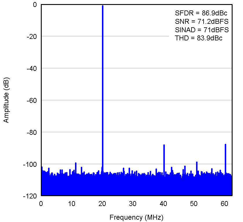 Figure 25. FFT for 20-MHz Input Signal
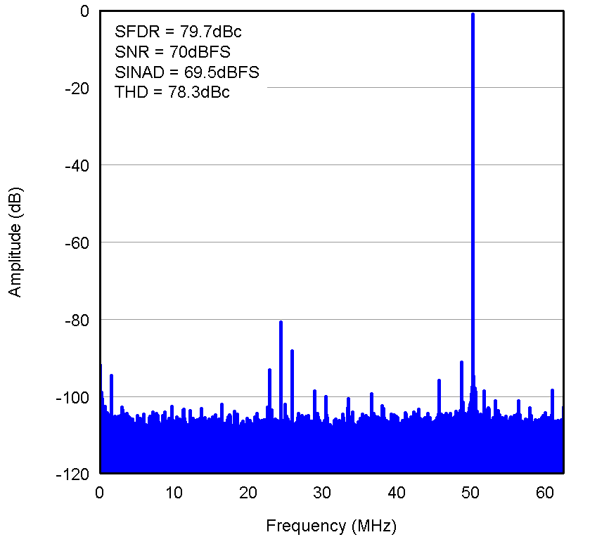 Figure 27. FFT for 300-MHz Input Signal
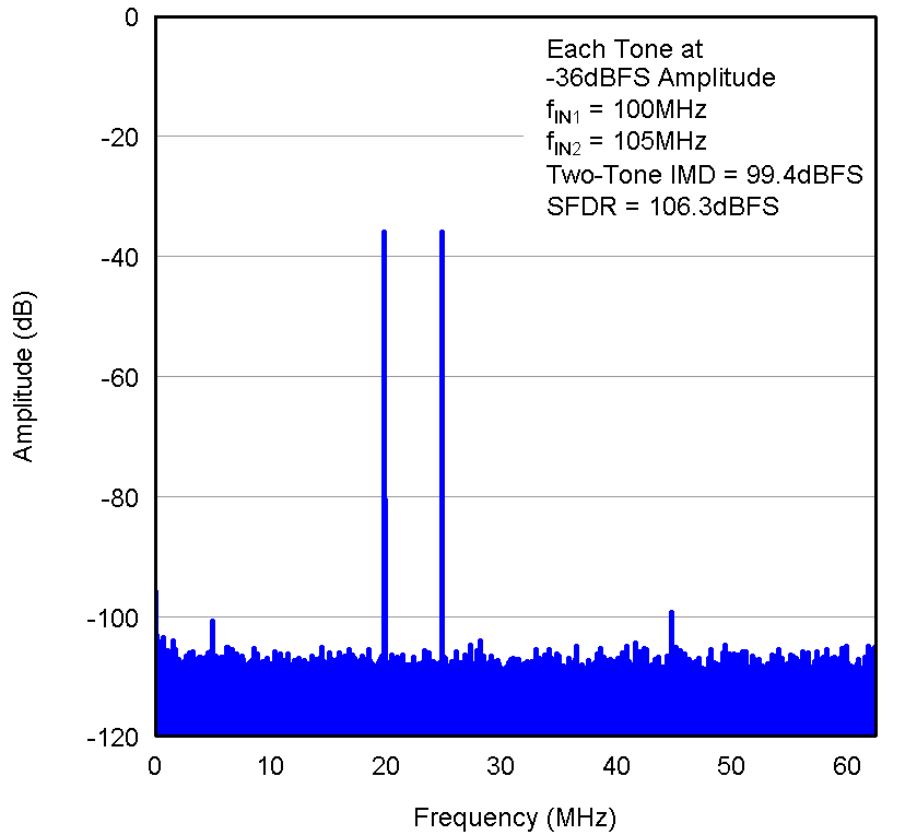 Figure 29. FFT for Two-Tone Input Signal
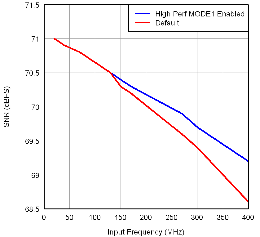 Figure 31. SNR vs Input Frequency
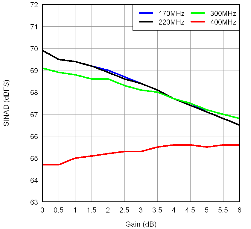 Figure 33. SINAD Across Gain and Input Frequency
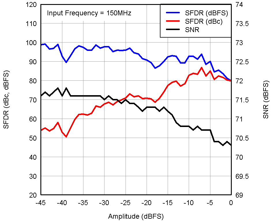 Figure 35. Performance Across Input Amplitude
 (Single Tone)
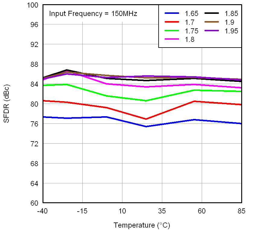 Figure 37. SFDR Across Temperature vs AVDD Supply
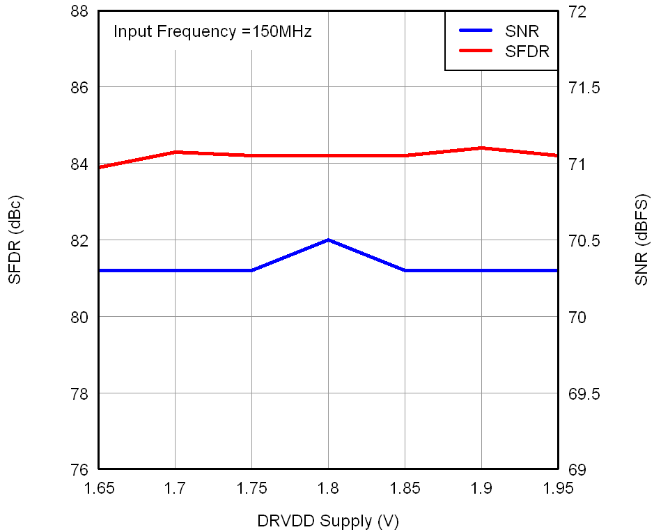 Figure 39. Performance Across DRVDD Supply Voltage
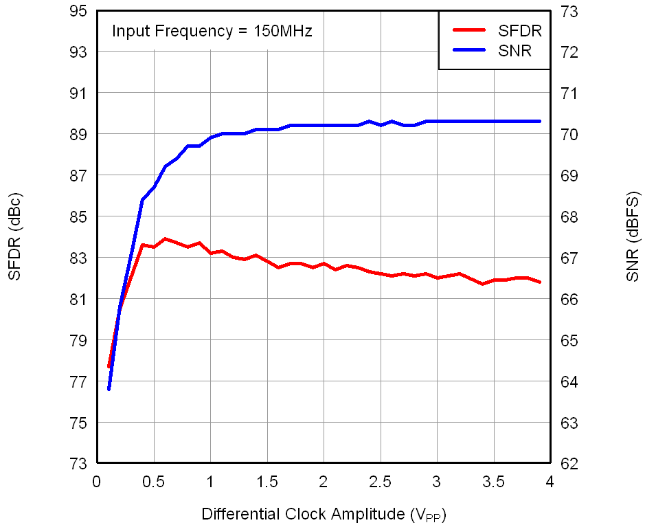 Figure 41. Performance Across Input Clock Amplitude
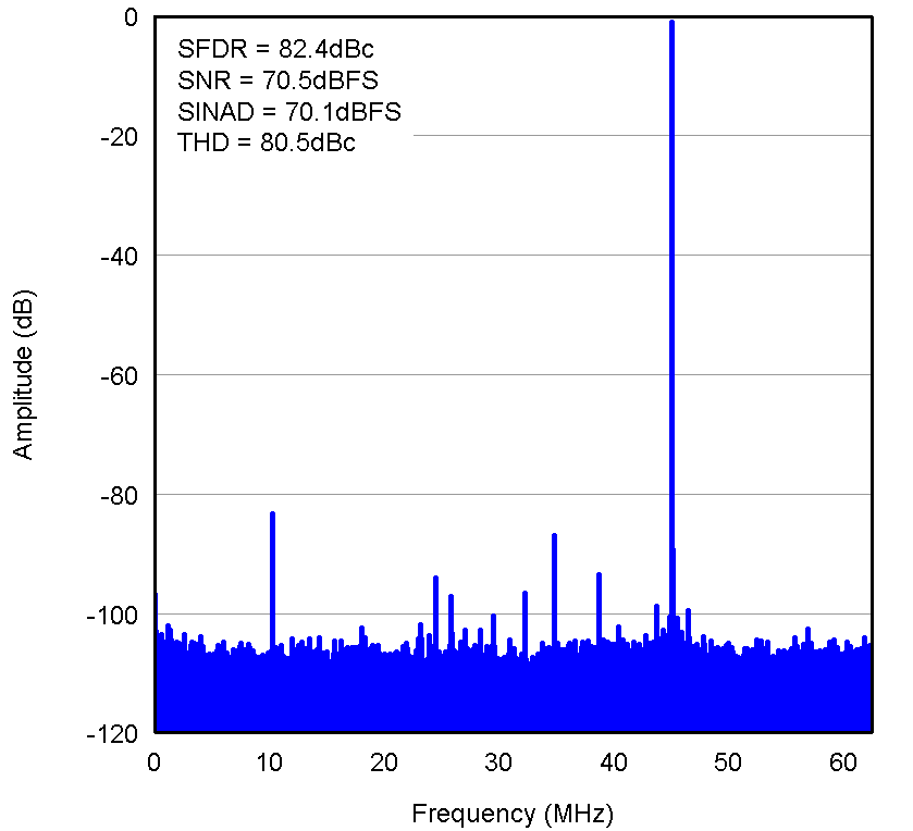 Figure 26. FFT for 170-MHz Input Signal
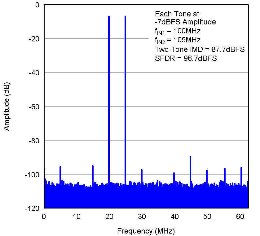 Figure 28. FFT for Two-Tone Input Signal
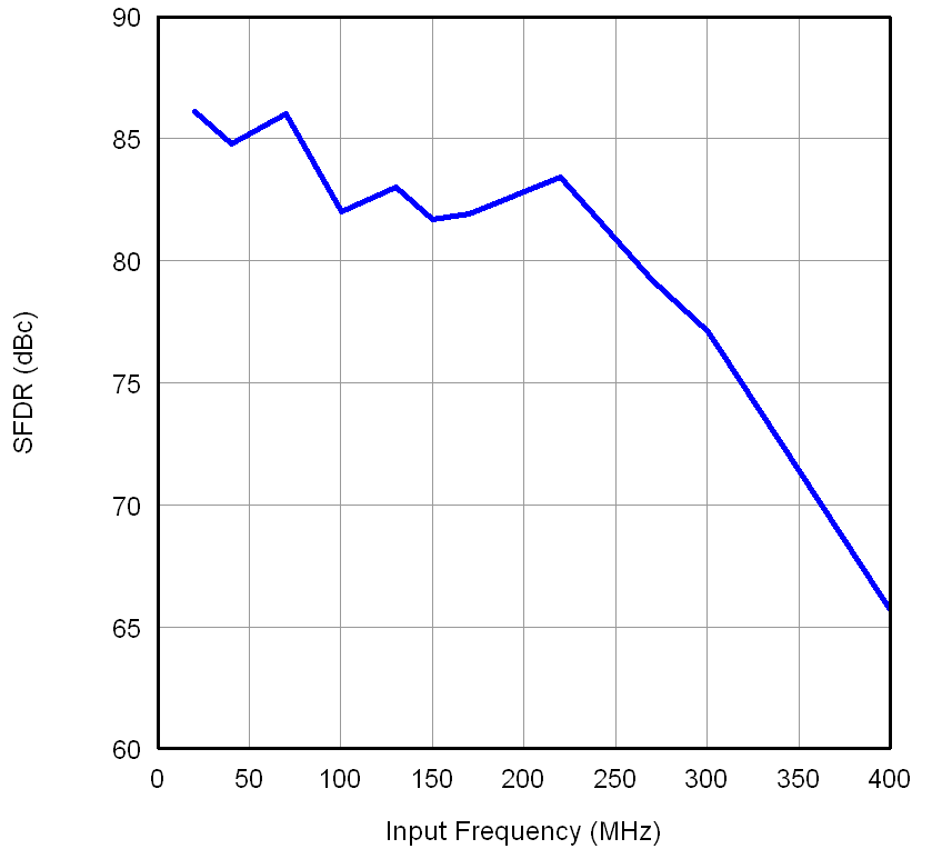 Figure 30. SFDR vs Input Frequency
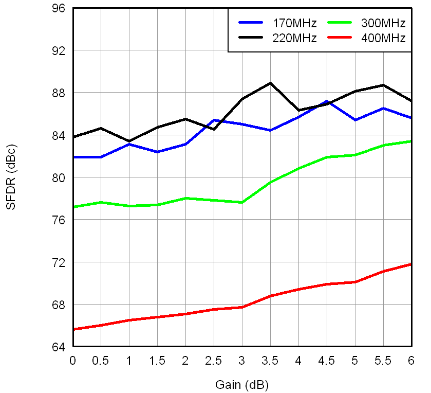 Figure 32. SFDR Across Gain and Input Frequency
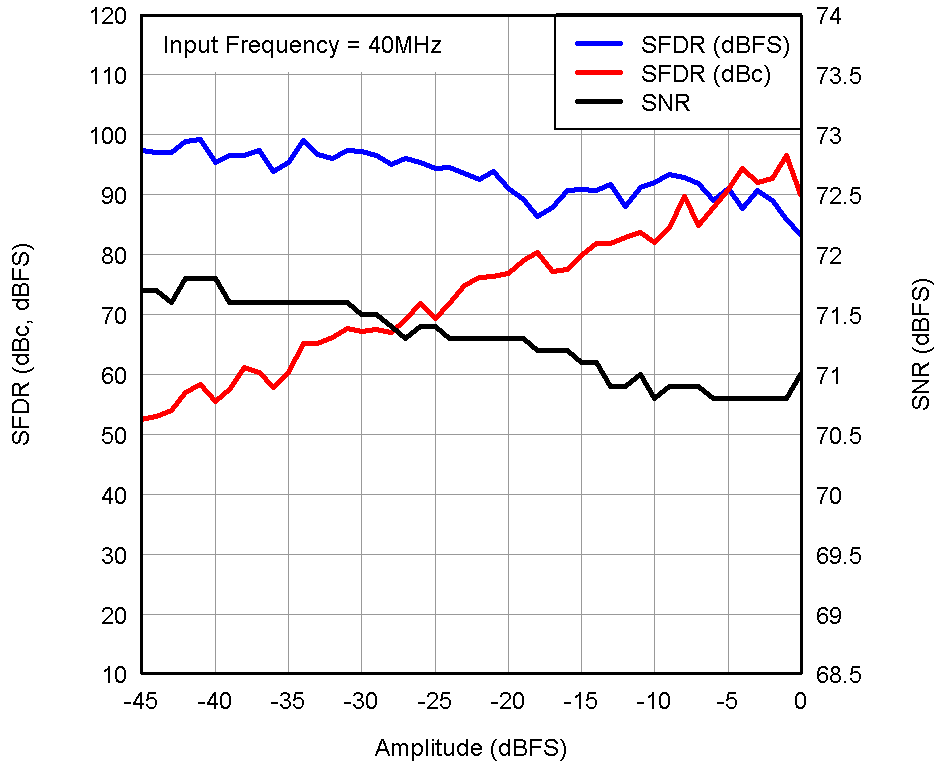 Figure 34. Performance Across Input Amplitude
(Single Tone)
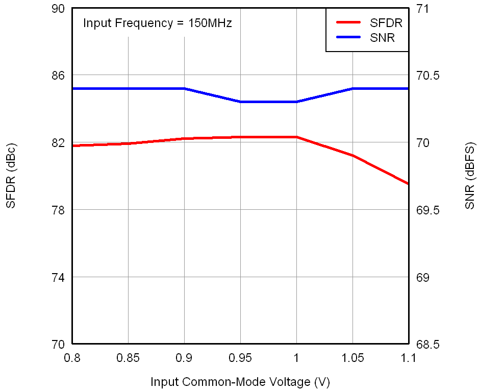 Figure 36. Performance vs Input Common-Mode Voltage
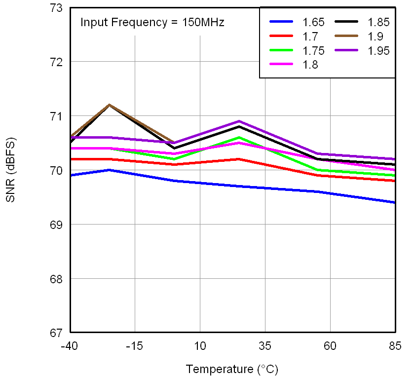 Figure 38. SNR Across Temperature vs AVDD Supply
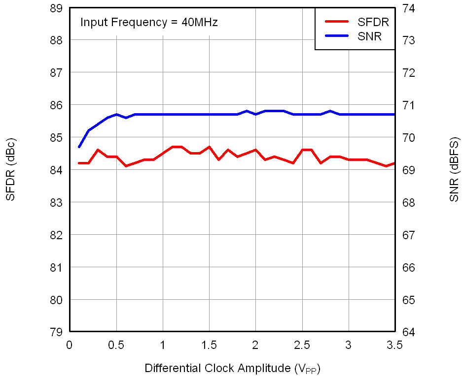 Figure 40. Performance Across Input Clock Amplitude
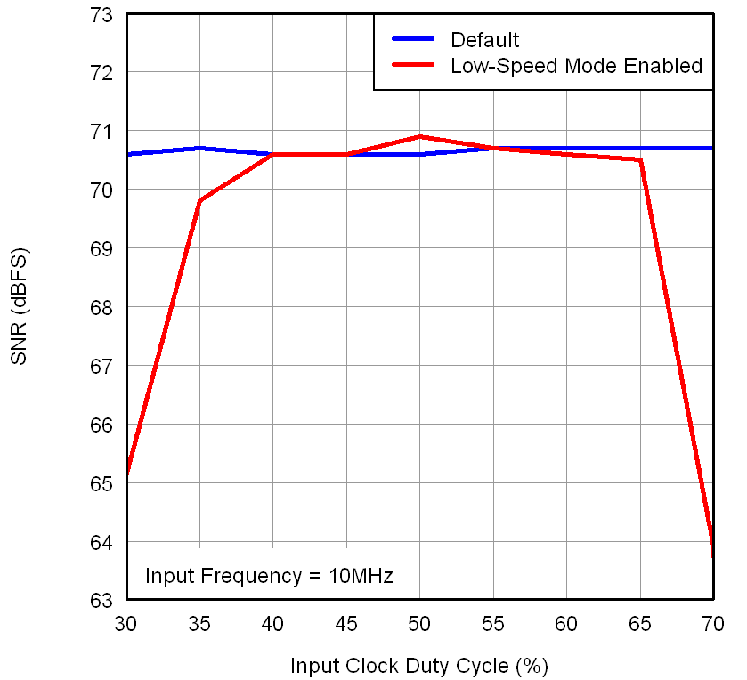 Figure 42. SNR Across Input Clock Duty Cycle
7.15 Typical Characteristics: ADS4142
At 25°C, AVDD = 1.8 V, DRVDD = 1.8 V, maximum-rated sampling frequency, sine wave input clock, 1.5-VPP differential clock amplitude, 50% clock duty cycle, –1-dBFS differential analog input, 0-dB gain, low-latency mode, DDR LVDS output interface, and 32k-point FFT, unless otherwise noted. Figure 43. FFT for 20-MHz Input Signal
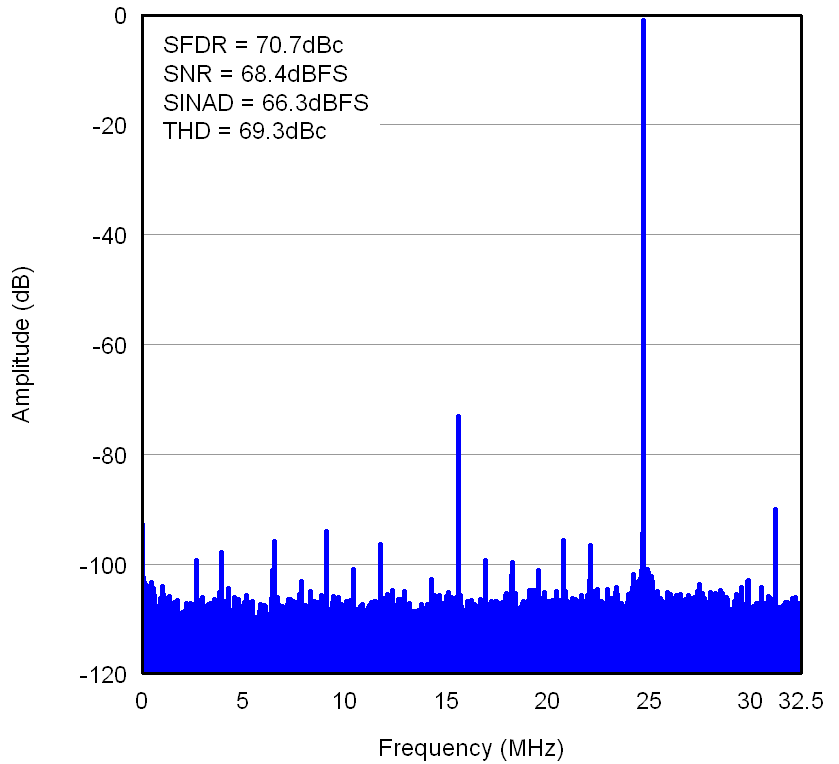 Figure 45. FFT for 300-MHz Input Signal
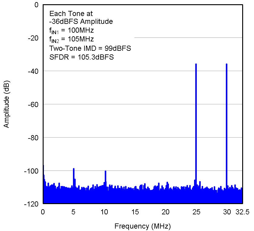 Figure 47. FFT for Two-Tone Input Signal
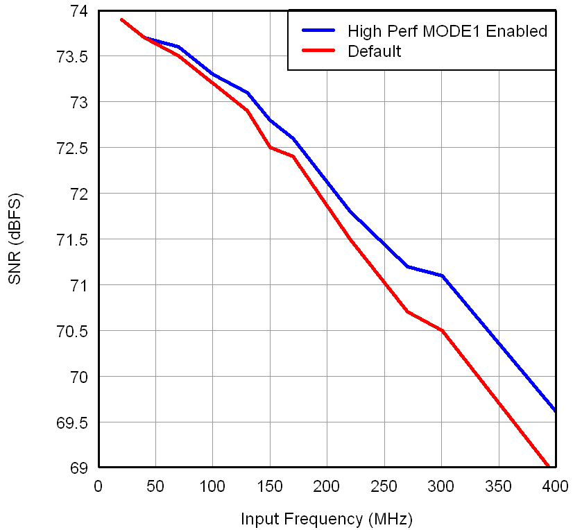 Figure 49. SNR vs Input Frequency
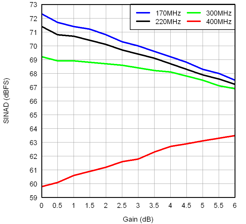 Figure 51. SINAD Across Gain and Input Frequency
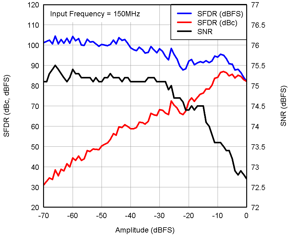 Figure 53. Performance Across Input Amplitude
(Single Tone)
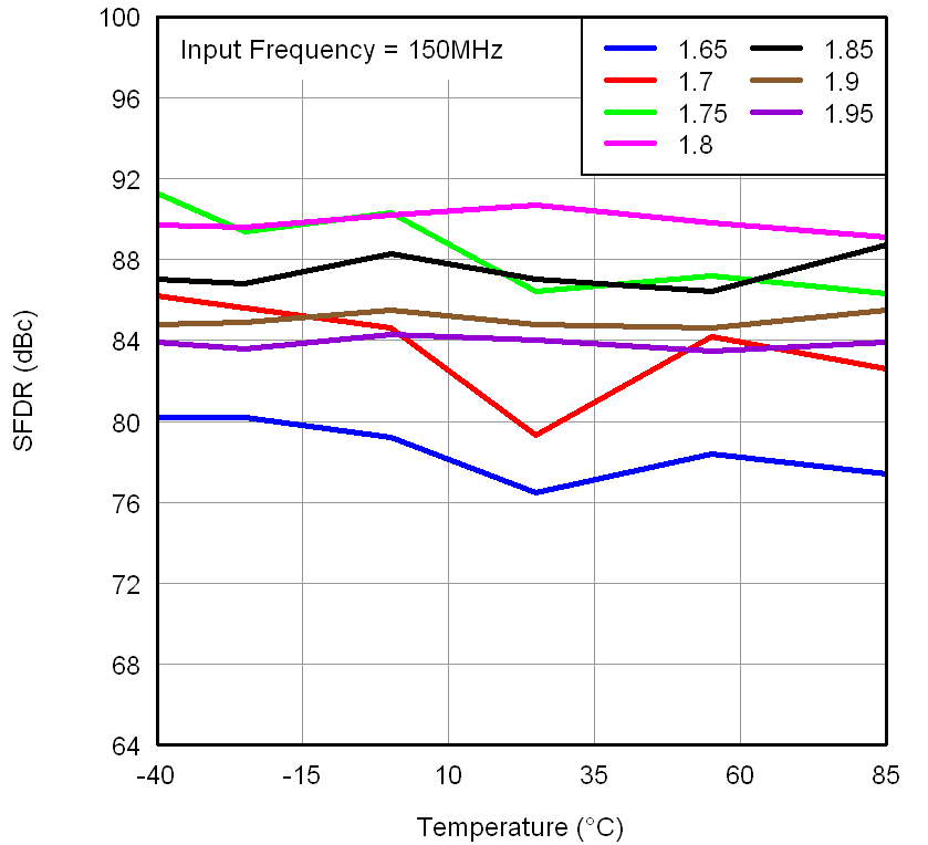 Figure 55. SFDR Across Temperature vs AVDD Supply
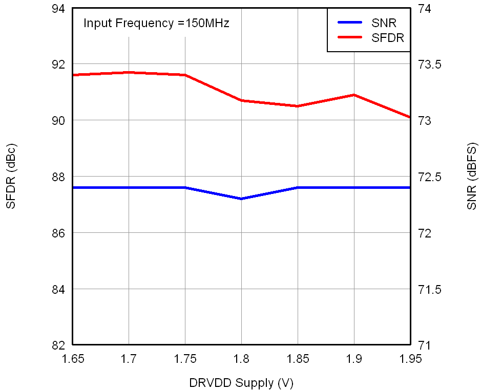 Figure 57. Performance Across DRVDD Supply Voltage
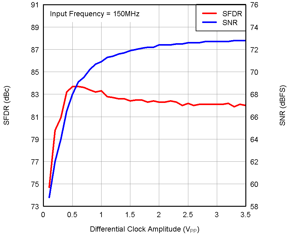 Figure 59. Performance Across Input Clock Amplitude
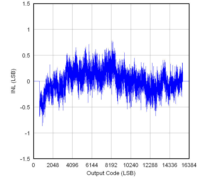 Figure 61. Integral Nonlinearity
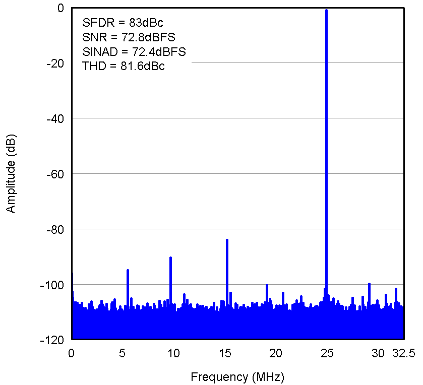 Figure 44. FFT for 170-MHz Input Signal
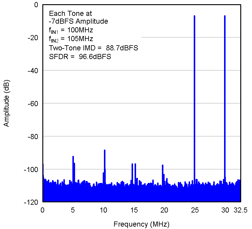 Figure 46. FFT for Two-Tone Input Signal
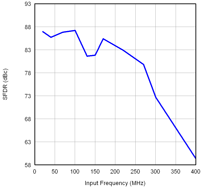 Figure 48. SFDR vs Input Frequency
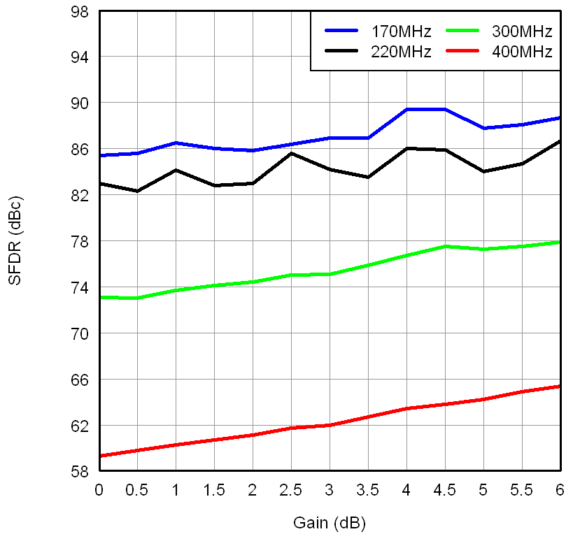 Figure 50. SFDR Across Gain and Input Frequency
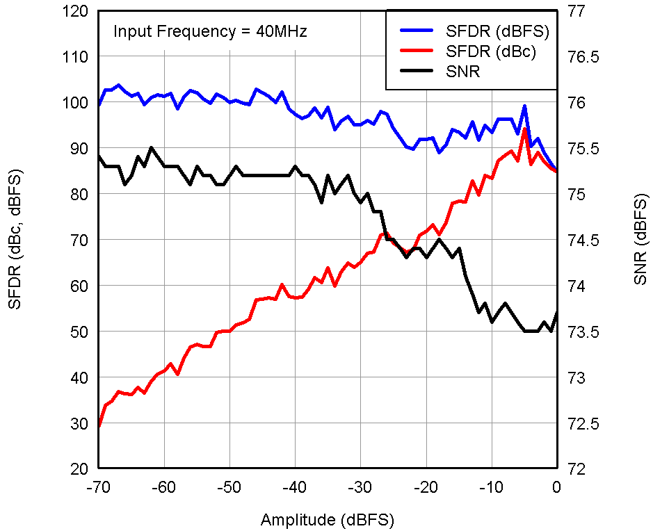 Figure 52. Performance Across Input Amplitude
 (Single Tone)
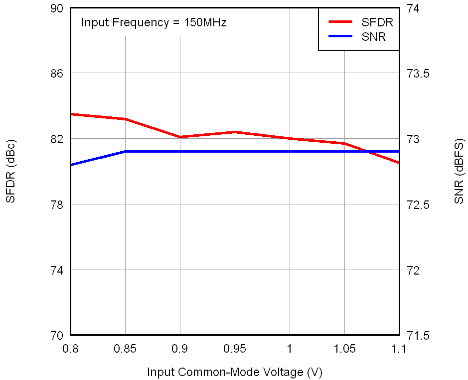 Figure 54. Performance vs Input Common-Mode Voltage
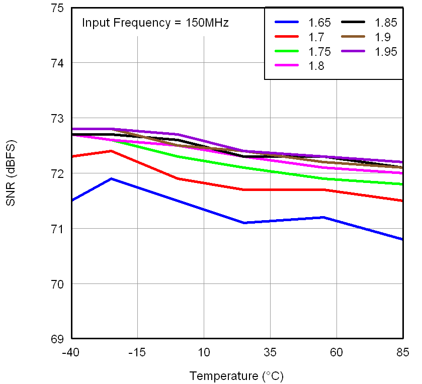 Figure 56. SNR Across Temperature vs AVDD Supply
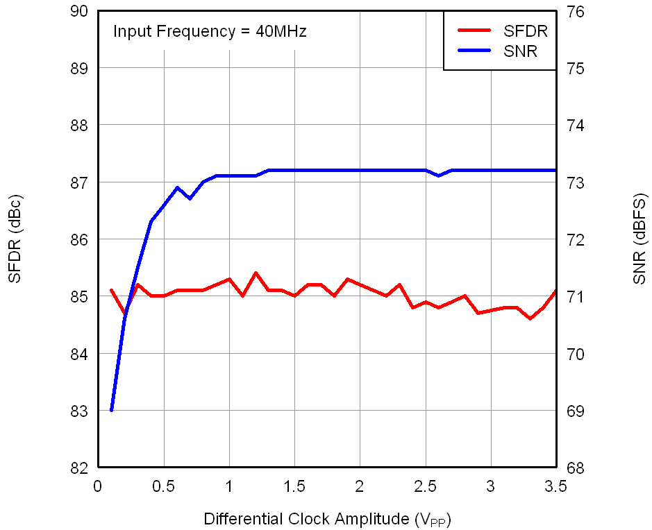 Figure 58. Performance Across Input Clock Amplitude
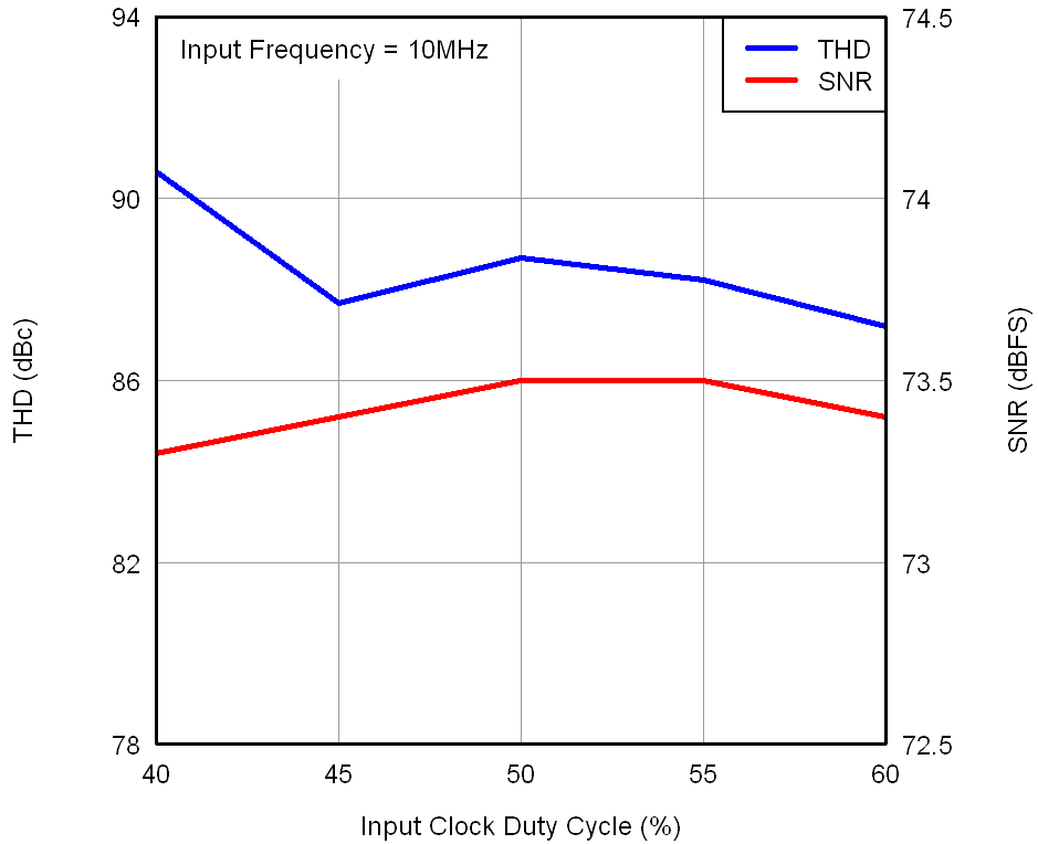 Figure 60. Performance Across Input Clock Duty Cycle
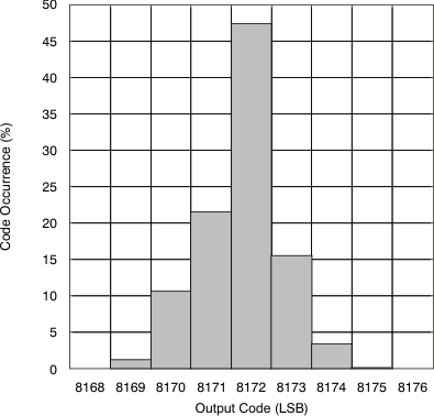 Figure 62. Output Noise Histogram
 (With Inputs Shorted to VCM)
7.16 Typical Characteristics: ADS4145
At 25°C, AVDD = 1.8 V, DRVDD = 1.8 V, maximum-rated sampling frequency, sine-wave input clock, 1.5-VPP differential clock amplitude, 50% clock duty cycle, –1-dBFS differential analog input, 0-dB gain, low-latency mode, DDR LVDS output interface, and 32k-point FFT, unless otherwise noted.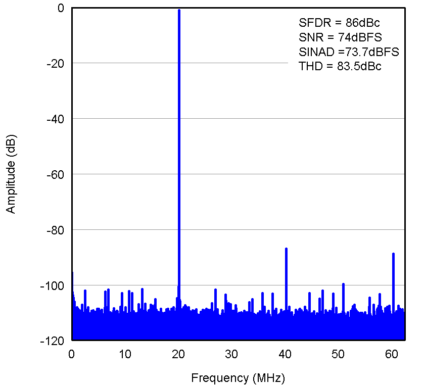 Figure 63. FFT for 20-MHz Input Signal
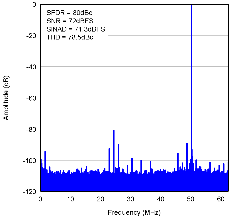 Figure 65. FFT for 300-MHz Input Signal
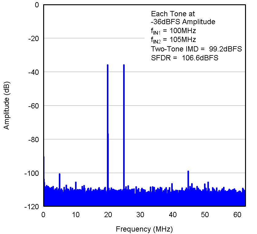 Figure 67. FFT for Two-Tone Input Signal
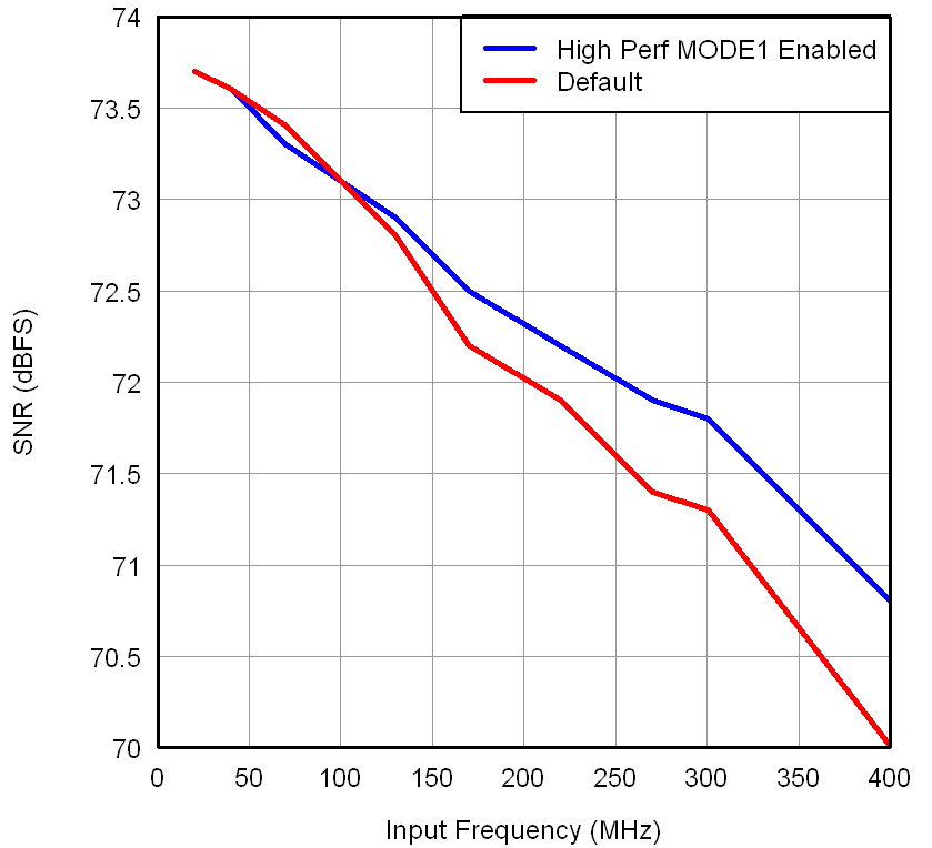 Figure 69. SNR vs Input Frequency
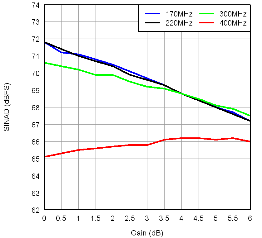 Figure 71. SINAD Across Gain and Input Frequency
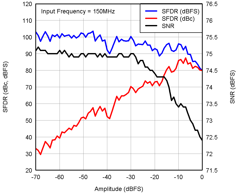 Figure 73. Performance Across Input Amplitude
 (Single Tone)
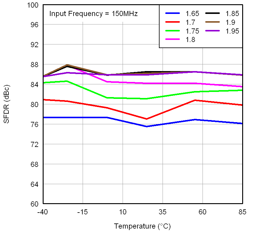 Figure 75. SFDR Across Temperature vs AVDD Supply
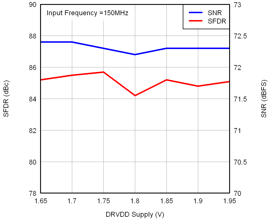 Figure 77. Performance Across DRVDD Supply Voltage
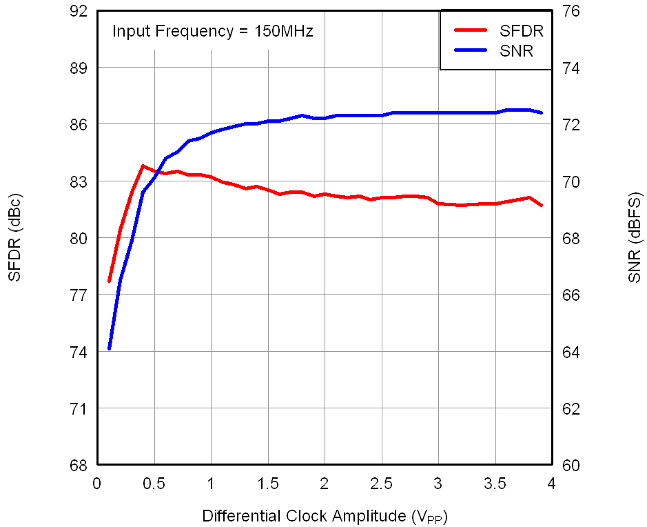 Figure 79. Performance Across Input Clock Amplitude
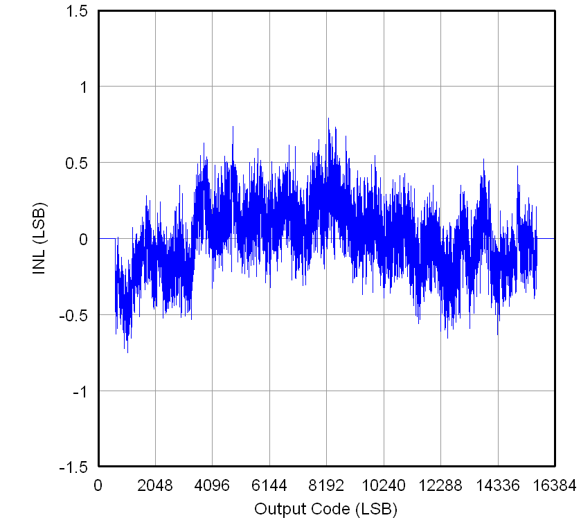 Figure 81. Integral Nonlinearity
 Figure 64. FFT for 170-MHz Input Signal
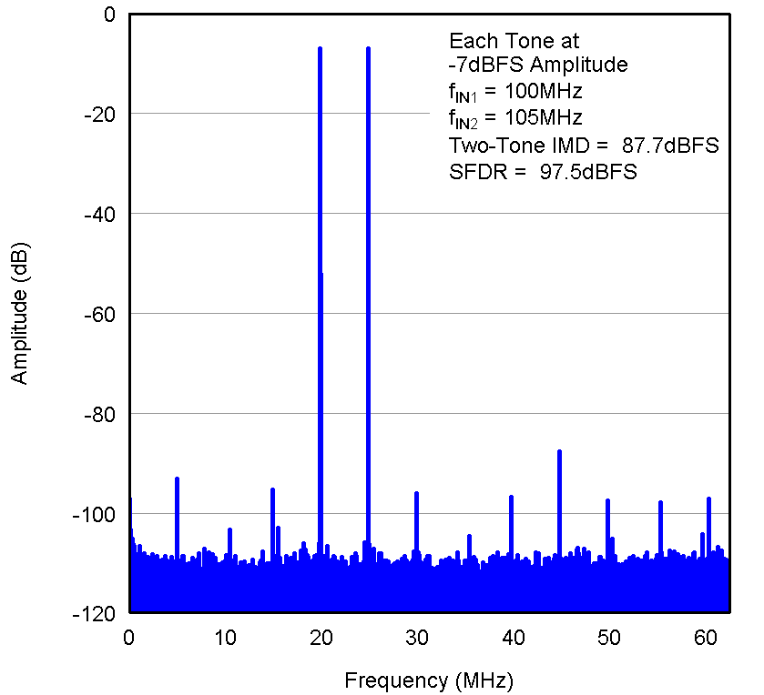 Figure 66. FFT for Two-Tone Input Signal
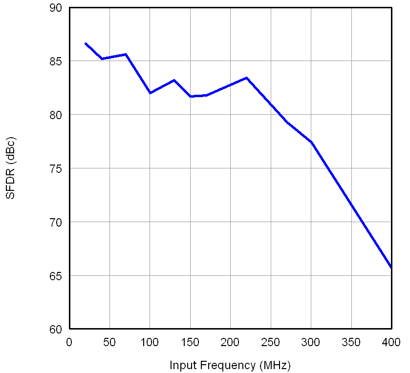 Figure 68. SFDR vs Input Frequency
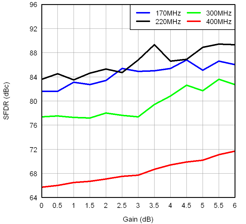 Figure 70. SFDR Across Gain and Input Frequency
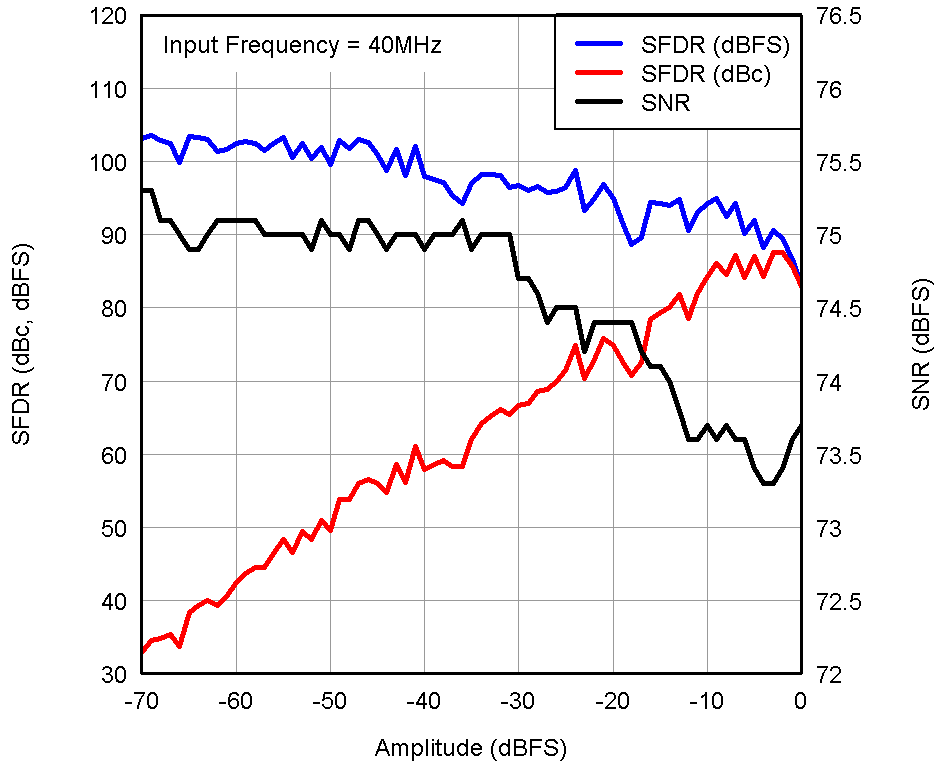 Figure 72. Performance Across Input Amplitude
(Single Tone)
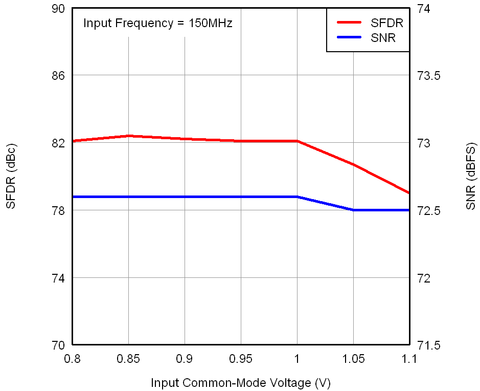 Figure 74. Performance vs Input Common-Mode Voltage
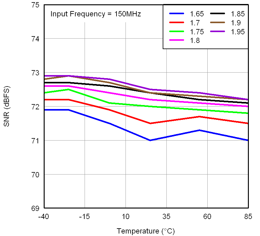 Figure 76. SNR Across Temperature vs AVDD Supply
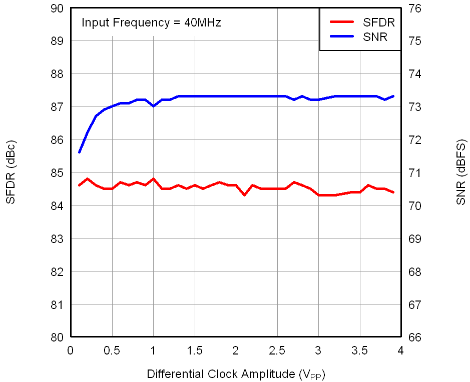 Figure 78. Performance Across Input Clock Amplitude
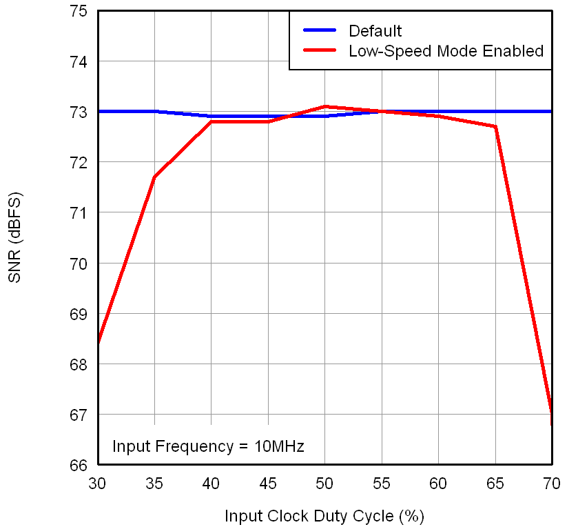 Figure 80. SNR Across Input Clock Duty Cycle
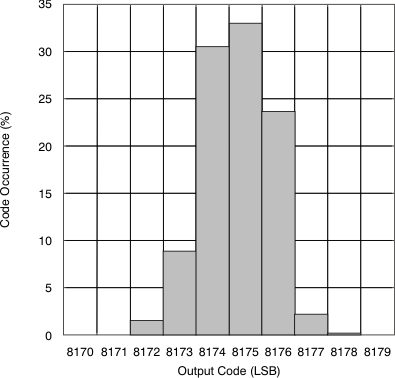 Figure 82. Output Noise Histogram
(With Inputs Shorted to VCM)
7.17 Typical Characteristics: Common
At 25°C, AVDD = 1.8 V, DRVDD = 1.8 V, maximum-rated sampling frequency, sine-wave input clock, 1.5-VPP differential clock amplitude, 50% clock duty cycle, –1-dBFS differential analog input, 0-dB gain, low-latency mode, DDR LVDS output interface, and 32k-point FFT, unless otherwise noted.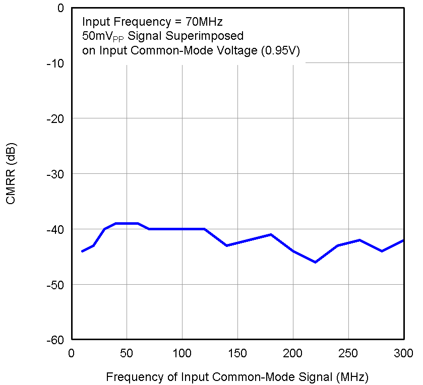 Figure 83. CMRR vs Frequency
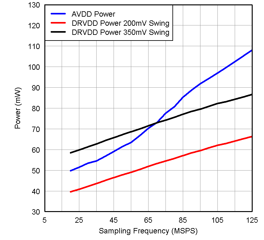 Figure 85. Power vs Sample Rate
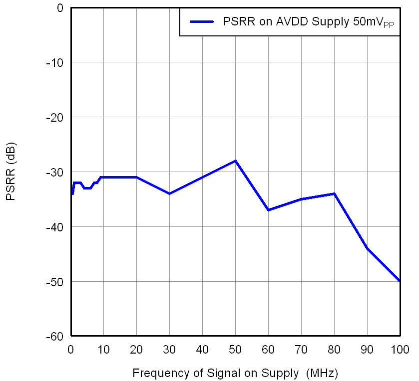 Figure 84. PSRR vs Frequency
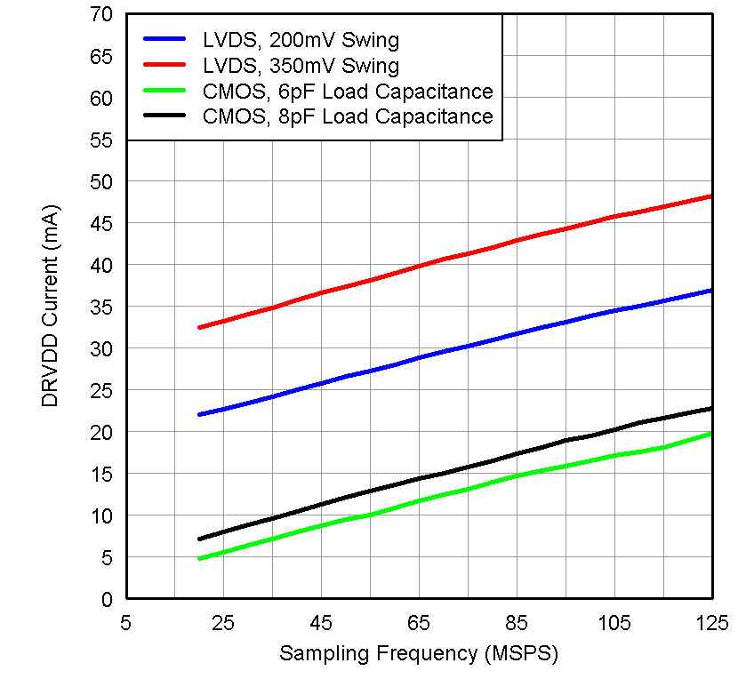 Figure 86. DRVDD Current vs Sample Rate
7.18 Typical Characteristics: Contour
At 25°C, AVDD = 1.8 V, DRVDD = 1.8 V, maximum-rated sampling frequency, sine-wave input clock, 1.5-VPP differential clock amplitude, 50% clock duty cycle, –1-dBFS differential analog input, 0-dB gain, low-latency mode, DDR LVDS output interface, and 32k-point FFT, unless otherwise noted.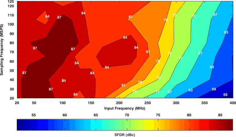 Figure 87. SFDR Across Input and Sampling Frequencies (0-dB Gain)
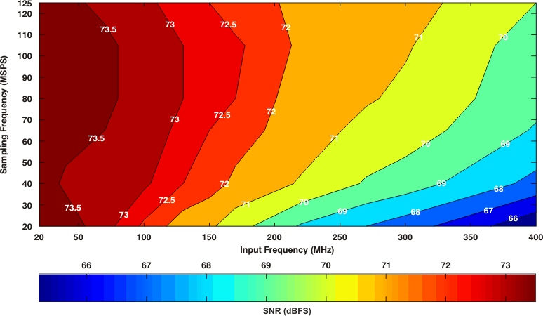 Figure 89. ADS414x: SNR ACROSS Input and Sampling Frequencies (0-dB Gain)
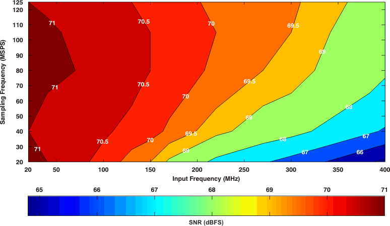 Figure 91. ADS412x SNR Across Input and Sampling Frequencies (0-dB Gain)
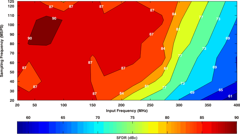 Figure 88. SFDR Across Input and Sampling Frequencies (6-dB Gain)
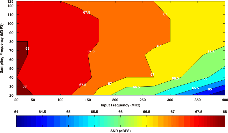 Figure 90. ADS414x: SNR Across Input and Sampling Frequencies (6-dB Gain)
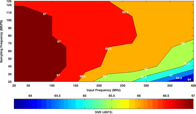 Figure 92. ADS412x SNR Across Input and Sampling Frequencies (6-dB Gain)
