-
ADS5474 14-Bit, 400-MSPS Analog-to-Digital Converter
- 1 Features
- 2 Applications
- 3 Description
- 4 Revision History
- 5 Pin Configuration and Functions
- 6 Specifications
- 7 Detailed Description
- 8 Application and Implementation
- 9 Power Supply Recommendations
- 10Layout
- 11Device and Documentation Support
- 12Mechanical, Packaging, and Orderable Information
- IMPORTANT NOTICE
Package Options
Mechanical Data (Package|Pins)
- PFP|80
Thermal pad, mechanical data (Package|Pins)
- PFP|80
Orderable Information
ADS5474 14-Bit, 400-MSPS Analog-to-Digital Converter
1 Features
- 400-MSPS Sample Rate
- 14-Bit Resolution, 11.2-Bits ENOB
- 1.4-GHz Input Bandwidth
- 80-dBc SFDR at 230 MHz and 400 MSPS
- 69.8-dBFS SNR at 230 MHz and 400 MSPS
- 2.2-VPP Differential Input Voltage
- LVDS-Compatible Outputs
- 2.5-W Total Power Dissipation
- 50-mW Power-Down Mode
- Offset Binary Output Format
- Output Data Transitions on the Rising and Falling Edges of a Half-Rate Output Clock
- On-Chip Analog Buffer, Track-and-Hold, and Reference Circuit
- HTQFP-80 PowerPAD™ Package
(14-mm × 14-mm Footprint) - Industrial Temperature Range:
–40°C to +85°C - Pin-Similar, -Compatible With 12-, 13-, and 14-Bit Family: ADS5463, ADS5440, ADS5444
2 Applications
- Test and Measurement Instrumentation
- Software-Defined Radio
- Data Acquisition
- Power Amplifier Linearization
- Communication Instrumentation
- Radar
3 Description
The ADS5474 device is a 14-bit, 400-MSPS analog-to-digital converter (ADC) that operates from both a 5-V supply and 3.3-V supply while providing LVDS-compatible digital outputs. This ADC is one of a family of 12-, 13-, and 14-bit ADCs that operate from 210 MSPS to 500 MSPS. The ADS5474 device has an input buffer that isolates the internal switching of the onboard track and hold (T&H) from disturbing the signal source while providing a high-impedance input. An internal reference generator is also provided to simplify the system design.
Designed with a 1.4-GHz input bandwidth for the conversion of wide-bandwidth signals that exceed 400 MHz of input frequency at 400 MSPS, the ADS5474 device has outstanding low-noise performance and spurious-free dynamic range over a large input frequency range.
The ADS5474 device is available in an TQFP-80 PowerPAD package. The device is built on Texas Instruments complementary bipolar process (BiCom3) and is specified over the full industrial temperature range (–40°C to +85°C).
Device Information(1)
| PART NUMBER | PACKAGE | BODY SIZE (NOM) |
|---|---|---|
| ADS5474 | HTQFP (80) | 12.00 mm x 12.00 mm |
- For all available packages, see the orderable addendum at the end of the data sheet.
Block Diagram

4 Revision History
Changes from C Revision (January 2016) to D Revision
- Changed CLK input sample rate (sine wave) parameter maximum specification from 400 MSPS to 404 MSPS Go
- Changed max sample rate from 400 MHz to 404 MHz in Detailed Design Procedure sectionGo
Changes from B Revision (February 2012) to C Revision
- Added ESD Ratings table, Feature Description section, Device Functional Modessection, Application and Implementation section, Power Supply Recommendations section, Layout section, Device and Documentation Support section, and Mechanical, Packaging, and Orderable Information section Go
Changes from A Revision (August 2008) to B Revision
5 Pin Configuration and Functions
Pin Functions
| PIN | DESCRIPTION | ||
|---|---|---|---|
| NAME | NO. | TYPE | |
| AIN | 16 | I | Differential input signal (positive) |
| AIN | 17 | I | Differential input signal (negative) |
| AVDD5 | 3 | Analog power supply (5 V) | |
| 8 | |||
| 13 | |||
| 14 | |||
| 19 | |||
| 21 | |||
| 23 | |||
| 25 | |||
| 27 | |||
| 31 | |||
| AVDD3 | 35 | Analog power supply (3.3 V) (suggestion for ≤ 250 MSPS: leave option to connect to 5 V for ADS5440, ADS5444 13-bit compatibility) | |
| 37 | |||
| 39 | |||
| DVDD3 | 1 | Digital and output driver power supply (3.3 V) | |
| 51 | |||
| 66 | |||
| AGND | 7 | Analog Ground | |
| 9 | |||
| 12 | |||
| 15 | |||
| 18 | |||
| 20 | |||
| 22 | |||
| 24 | |||
| 26 | |||
| 28 | |||
| 30 | |||
| 32 | |||
| 34 | |||
| 36 | |||
| 38 | |||
| 40 | |||
| DGND | 2 | Digital Ground | |
| 52 | |||
| 65 | |||
| CLK | 10 | I | Differential input clock (positive). Conversion is initiated on rising edge, digital outputs on falling edge. |
| CLK | 11 | I | Differential input clock (negative) |
| D0 | 48 | O | LVDS digital output pair, least significant bit (LSB) |
| D0 | 47 | ||
| D1 | 50 | O | LVDS digital output pairs |
| D1 | 49 | ||
| D2 | 54 | ||
| D2 | 53 | ||
| D3 | 56 | ||
| D3 | 55 | ||
| D4 | 58 | ||
| D4 | 57 | ||
| D5 | 60 | ||
| D5 | 59 | ||
| D6 | 62 | ||
| D6 | 61 | ||
| D7 | 64 | ||
| D7 | 63 | ||
| D8 | 68 | ||
| D8 | 67 | ||
| D9 | 70 | ||
| D9 | 69 | ||
| D10 | 72 | ||
| D10 | 71 | ||
| D11 | 74 | ||
| D11 | 73 | ||
| D12 | 76 | ||
| D12 | 75 | ||
| D13 | 78 | O | LVDS digital output pair, most significant bit (MSB) |
| D13 | 77 | ||
| DRY | 80 | O | Data ready LVDS output pair |
| DRY | 79 | ||
| NC | 4 | - | No connection (pins 4 and 5 should be left floating) |
| 5 | |||
| 43 | - | No connection (pins 43 to 46 are possible future bit additions for this pinout and therefore can be connected to a digital bus or left floating) | |
| 44 | |||
| 45 | |||
| 46 | |||
| OVR | 42 | O | Overrange indicator LVDS output. A logic high signals an analog input in excess of the full-scale range. |
| OVR | 41 | ||
| VCM | 29 | O | Common-mode voltage output (3.1 V nominal). Commonly used in DC-coupled applications to set the input signal to the correct common-mode voltage. A 0.1-μF capacitor from VCM to AGND is recommended, but not required. (This pin is not used on the ADS5440, ADS5444, and ADS5463) |
| PWD | 33 | Power-down (active high). Device is in sleep mode when PWD pin is logic HIGH. ADC converter is awake when PWD is logic LOW (grounded). (This pin is not used on the ADS5440, ADS5444, and ADS5463) |
|
| VREF | 6 | Reference voltage input/output (2.4 V nominal). A 0.1-μF capacitor from VREF to AGND is recommended, but not required. | |
| (Power Pad) | (not numbered) | Power Pad for thermal relief, also Analog Ground | |
6 Specifications
6.1 Absolute Maximum Ratings
over operating free-air temperature range, unless otherwise noted.(1)| MIN | MAX | UNIT | ||
|---|---|---|---|---|
| Supply voltage | AVDD5 to GND | 6 | V | |
| AVDD3 to GND | 5 | |||
| DVDD3 to GND | 5 | |||
| Analog input to GND | Valid when supplies are on and within normal ranges. See additional information in the Power Supplies portion of the applications information in the back of the datasheet regarding Clock and Analog Inputs when the supplies are off. | –0.3 | (AVDD5 + 0.3) | V |
| Clock input to GND | –0.3 | (AVDD5 + 0.3) | V | |
| CLK to CLK | –2.5 | 2.5 | V | |
| Digital data output to GND | –0.3 | (DVDD3 + 0.3) | V | |
| Operating temperature range | –40 | 85 | °C | |
| Maximum junction temperature | +150 | °C | ||
| Storage temperature range | –65 | 150 | °C | |
6.2 ESD Ratings
| VALUE | UNIT | |||
|---|---|---|---|---|
| V(ESD) | Electrostatic discharge | Human-body model (HBM), per ANSI/ESDA/JEDEC JS-001(1) | 2000 | V |
6.3 Recommended Operating Conditions
| MIN | NOM | MAX | UNIT | ||
|---|---|---|---|---|---|
| SUPPLIES | |||||
| AVDD5 | Analog supply voltage | 4.75 | 5 | 5.25 | V |
| AVDD3 | Analog supply voltage | 3.1 | 3.3 | 3.6 | V |
| DVDD3 | Output driver supply voltage | 3 | 3.3 | 3.6 | V |
| ANALOG INPUT | |||||
| Differential input range | 2.2 | VPP | |||
| VCM | Input common mode | 3.1 | V | ||
| DIGITAL OUTPUT (DRY, DATA, OVR) | |||||
| Maximum differential output load | 10 | pF | |||
| CLOCK INPUT (CLK) | |||||
| CLK input sample rate (sine wave) | 20 | 404 | MSPS | ||
| Clock amplitude, differential sine wave (see Figure 37) | 0.5 | 5 | VPP | ||
| Clock duty cycle (see Figure 31) | 40% | 50% | 60% | ||
| TA | Operating free-air temperature | –40 | +85 | °C | |
6.4 Thermal Information
| THERMAL METRIC(1) | ADS5474 | UNIT | |
|---|---|---|---|
| PFP (HTQFP) | |||
| 80 PINS | |||
| RθJA | Junction-to-ambient thermal resistance | 25.9 | °C/W |
| RθJC(top) | Junction-to-case (top) thermal resistance | 7.6 | °C/W |
| RθJB | Junction-to-board thermal resistance | 9.8 | °C/W |
| ψJT | Junction-to-top characterization parameter | 0.2 | °C/W |
| ψJB | Junction-to-board characterization parameter | 9.7 | °C/W |
| RθJC(bot) | Junction-to-case (bottom) thermal resistance | 0.2 | °C/W |
6.5 Electrical Characteristics
Typical values at TA = 25°C: minimum and maximum values over full temperature range TMIN = –40°C to TMAX = 85°C, sampling rate = 400 MSPS, 50% clock duty cycle, AVDD5 = 5 V, AVDD3 = 3.3 V, DVDD3 = 3.3 V, –1 dBFS differential input, and 3-VPP differential clock, unless otherwise noted.| PARAMETER | TEST CONDITIONS | MIN | TYP | MAX | UNIT | |
|---|---|---|---|---|---|---|
| Resolution | 14 | Bits | ||||
| ANALOG INPUTS | ||||||
| Differential input range | 2.2 | VPP | ||||
| Analog input common-mode voltage | Self-biased; see VCM specification below | 3.1 | V | |||
| Input resistance (dc) | Each input to VCM | 500 | Ω | |||
| Input capacitance | Each input to GND | 2.3 | pF | |||
| Analog input bandwidth (–3dB) | 1.44 | GHz | ||||
| CMRR | Common-mode rejection ratio | Common-mode signal < 50 MHz (see Figure 27) |
100 | dB | ||
| INTERNAL REFERENCE VOLTAGE | ||||||
| VREF | Reference voltage | 2.4 | V | |||
| VCM | Analog input common-mode voltage reference output | With internal VREF. Provided as an output via the VCM pin for dc-coupled applications. If an external VREF is used, the VCM pin tracks as illustrated in Figure 42 | 2.9 | 3.1 | 3.3 | V |
| VCM temperature coefficient | –0.8 | mV/°C | ||||
| DYNAMIC ACCURACY | ||||||
| No missing codes | Assured | |||||
| DNL | Differential linearity error | fIN = 70 MHz | –0.99 | ±0.7 | 1.5 | LSB |
| INL | Integral linearity error | fIN = 70 MHz | –3 | ±1 | 3 | LSB |
| Offset error | –11 | 11 | mV | |||
| Offset temperature coefficient | 0.02 | mV/°C | ||||
| Gain error | –5 | 5 | %FS | |||
| Gain temperature coefficient | –0.02 | %FS/°C | ||||
| POWER SUPPLY | ||||||
| IAVDD5 | 5-V analog supply current | VIN = full-scale, fIN = 70 MHz, fS = 400 MSPS |
338 | 372 | mA | |
| IAVDD3 | 3.3-V analog supply current | VIN = full-scale, fIN = 70 MHz, fS = 400 MSPS |
185 | 201 | mA | |
| IDVDD3 | 3.3-V digital supply current (includes LVDS) |
VIN = full-scale, fIN = 70 MHz, fS = 400 MSPS |
75 | 83 | mA | |
| Total power dissipation | 2.5 | 2.797 | W | |||
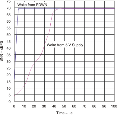
| Power-up time | From turn-on of AVDD5 | 50 | μs | |||
| Wake-up time | From PWD pin switched from HIGH (PWD active) to LOW (ADC awake) (see Figure 28) |
5 | μs | |||
| Power-down power dissipation | PWD pin = logic HIGH | 50 | 350 | mW | ||
| PSRR | Power-supply rejection ratio, AVDD5 supply |
Without 0.1-μF board supply capacitors, with < 1-MHz supply noise (see Figure 46) | 75 | dB | ||
| PSRR | Power-supply rejection ratio, AVDD3 supply |
Without 0.1-μF board supply capacitors, with < 1-MHz supply noise (see Figure 46) | 90 | dB | ||
| PSRR | Power-supply rejection ratio, DVDD3 supply |
Without 0.1-μF board supply capacitors, with < 1-MHz supply noise (see Figure 46) | 110 | dB | ||
| DYNAMIC AC CHARACTERISTICS | ||||||
| SNR | Signal-to-noise ratio | fIN = 30 MHz | 70.3 | dBFS | ||
| fIN = 70 MHz | 68.3 | 70.2 | ||||
| fIN = 130 MHz | 70.1 | |||||
| fIN = 230 MHz | 68 | 69.8 | ||||
| fIN = 351 MHz | 69.1 | |||||
| fIN = 451 MHz | 68.4 | |||||
| fIN = 651 MHz | 67.5 | |||||
| fIN = 751 MHz | 66.6 | |||||
| fIN = 999 MHz | 64.7 | |||||
| SFDR | Spurious-free dynamic range | fIN = 30 MHz | 88 | dBc | ||
| fIN = 70 MHz | 74 | 86 | ||||
| fIN = 130 MHz | 80 | |||||
| fIN = 230 MHz | 71 | 80 | ||||
| fIN = 351 MHz | 76 | |||||
| fIN = 451 MHz | 71 | |||||
| fIN = 651 MHz | 60 | |||||
| fIN = 751 MHz | 55 | |||||
| fIN = 999 MHz | 46 | |||||
| HD2 | Second-harmonic | fIN = 30 MHz | 89 | dBc | ||
| fIN = 70 MHz | 87 | |||||
| fIN = 130 MHz | 90 | |||||
| fIN = 230 MHz | 84 | |||||
| fIN = 351 MHz | 76 | |||||
| fIN = 451 MHz | 71 | |||||
| fIN = 651 MHz | 74 | |||||
| fIN = 751 MHz | 70 | |||||
| fIN = 999 MHz | 55 | |||||
| HD3 | Third-harmonic | fIN = 30 MHz | 93 | dBc | ||
| fIN = 70 MHz | 86 | |||||
| fIN = 130 MHz | 80 | |||||
| fIN = 230 MHz | 80 | |||||
| fIN = 351 MHz | 85 | |||||
| fIN = 451 MHz | 71 | |||||
| fIN = 651 MHz | 60 | |||||
| fIN = 751 MHz | 55 | |||||
| fIN = 999 MHz | 46 | |||||
| Worst harmonic, spur (other than HD2 and HD3) |
fIN = 30 MHz | 95 | dBc | |||
| fIN = 70 MHz | 93 | |||||
| fIN = 130 MHz | 85 | |||||
| fIN = 230 MHz | 85 | |||||
| fIN = 351 MHz | 87 | |||||
| fIN = 451 MHz | 87 | |||||
| fIN = 651 MHz | 90 | |||||
| fIN = 751 MHz | 87 | |||||
| fIN = 999 MHz | 80 | |||||
| THD | Total harmonic distortion | fIN = 30 MHz | 86 | dBc | ||
| fIN = 70 MHz | 83 | |||||
| fIN = 130 MHz | 78 | |||||
| fIN = 230 MHz | 77 | |||||
| fIN = 351 MHz | 75 | |||||
| fIN = 451 MHz | 68 | |||||
| fIN = 651 MHz | 60 | |||||
| fIN = 751 MHz | 55 | |||||
| fIN = 999 MHz | 45 | |||||
| SINAD | Signal-to-noise and distortion | fIN = 30 MHz | 69.2 | dBc | ||
| fIN = 70 MHz | 67 | 68.9 | ||||
| fIN = 130 MHz | 68.5 | |||||
| fIN = 230 MHz | 65.5 | 68.2 | ||||
| fIN = 351 MHz | 67.3 | |||||
| fIN = 451 MHz | 64.8 | |||||
| fIN = 651 MHz | 58.5 | |||||
| fIN = 751 MHz | 54 | |||||
| fIN = 999 MHz | 45.4 | |||||
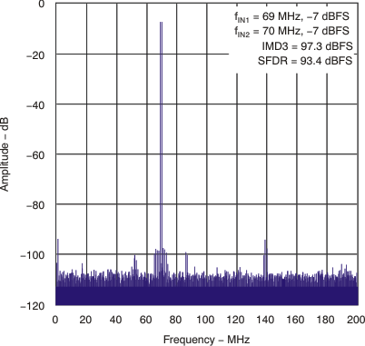
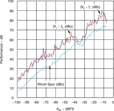
| Two-tone SFDR | fIN1 = 69 MHz, fIN2 = 70 MHz, each tone at –7 dBFS |
93 | dBFS | |||
| fIN1 = 69 MHz, fIN2 = 70 MHz, each tone at –16 dBFS |
95 | |||||
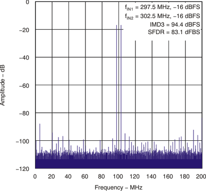
| fIN1 = 297.5 MHz, fIN2 = 302.5 MHz, each tone at –7 dBFS |
85 | |||||
| fIN1 = 297.5 MHz, fIN2 = 302.5 MHz, each tone at –16 dBFS |
83 | |||||
| ENOB | Effective number of bits | fIN = 70 MHz | 10.8 | 11.2 | Bits | |
| fIN = 230 MHz | 10.6 | 10.9 | ||||
| RMS idle-channel noise | Inputs tied to common-mode | 1.8 | LSB | |||
| DIGITAL OUTPUTS | ||||||
| VOD | Differential output voltage (±) | 247 | 350 | 454 | mV | |
| VOC | Common-mode output voltage | 1.125 | 1.375 | V | ||
| DIGITAL INPUTS | ||||||
| VIH | High level input voltage | PWD (pin 33) | 2 | V | ||
| VIL | Low level input voltage | PWD (pin 33) | 0.8 | V | ||
| IIH | High level input current | PWD (pin 33) | 1 | μA | ||
| IIL | Low level input current | PWD (pin 33) | –1 | μA | ||
| Input capacitance | PWD (pin 33) | 2 | pF | |||
6.6 Timing Characteristics
Typical values at TA = 25°C: minimum and maximum values over full temperature range TMIN = –40°C to TMAX = 85°C, sampling rate = 400 MSPS, 50% clock duty cycle, AVDD5 = 5 V, AVDD3 = 3.3 V, DVDD3 = 3.3 V, and 3-VPP differential clock, unless otherwise noted.(1)| TEST CONDITIONS | MIN | NOM | MAX | UNIT | ||
|---|---|---|---|---|---|---|
| ta | Aperture delay | 200 | ps | |||
| Aperture jitter, rms | Internal jitter of the ADC | 103 | fs | |||
| Latency | 3.5 | cycles | ||||
| tCLK | Clock period | 2.5 | 50 | ns | ||
| tCLKH | Clock pulse duration, high | 1 | ns | |||
| tCLKL | Clock pulse duration, low | 1 | ns | |||
| tDRY | CLK to DRY delay(2) | Zero crossing, 10-pF parasitic loading to GND on each output pin | 1000 | 1400 | 1800 | ps |
| tDATA | CLK to DATA/OVR delay(2) | Zero crossing, 10-pF parasitic loading to GND on each output pin | 800 | 1400 | 2000 | ps |
| tSKEW | DATA to DRY skew | tDATA – tDRY, 10-pF parasitic loading to GND on each output pin | –500 | 0 | 500 | ps |
| tRISE | DRY/DATA/OVR rise time | 10-pF parasitic loading to GND on each output pin | 500 | ps | ||
| tFALL | DRY/DATA/OVR fall time | 10-pF parasitic loading to GND on each output pin | 500 | ps | ||

6.7 Typical Characteristics
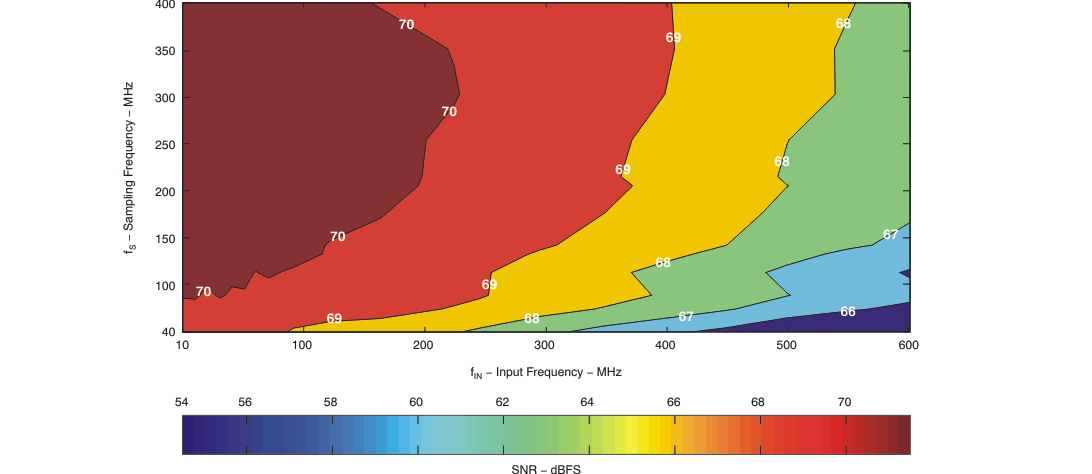
At TA = 25°C, sampling rate = 400 MSPS, 50% clock duty cycle, 3-VPP differential sinusoidal clock, analog input amplitude = –1 dBFS, AVDD5 = 5 V, AVDD3 = 3.3 V, and DVDD3 = 3.3 V, unless otherwise noted.


