SBAS556B October 2013 – August 2014 ADS7254 , ADS7854 , ADS8354
PRODUCTION DATA.
- 1 Features
- 2 Applications
- 3 Description
- 4 Revision History
- 5 Device Comparison Table
- 6 Pin Configurations and Functions
-
7 Specifications
- 7.1 Absolute Maximum Ratings
- 7.2 Handling Ratings
- 7.3 Recommended Operating Conditions
- 7.4 Thermal Information
- 7.5 Electrical Characteristics: ADS8354
- 7.6 Electrical Characteristics: ADS7854
- 7.7 Electrical Characteristics: ADS7254
- 7.8 Electrical Characteristics: All Devices
- 7.9 Timing Requirements: Interface Mode
- 7.10 Timing Characteristics: Serial Interface
- 7.11 Typical Characteristics: ADS8354
- 7.12 Typical Characteristics: ADS7854
- 7.13 Typical Characteristics: ADS7254
- 7.14 Typical Characteristics: Common to ADS8354, ADS7854, and ADS7254
-
8 Detailed Description
- 8.1 Overview
- 8.2 Functional Block Diagram
- 8.3 Feature Description
- 8.4 Device Functional Modes
- 8.5 Register Maps and Serial Interface
- 9 Application and Implementation
- 10Power-Supply Recommendations
- 11Layout
- 12Device and Documentation Support
- 13Mechanical, Packaging, and Orderable Information
Package Options
Mechanical Data (Package|Pins)
Thermal pad, mechanical data (Package|Pins)
- RTE|16
Orderable Information
1 Features
- 16-, 14-, and 12-Bit, Pin-Compatible Family
- Simultaneous Sampling of Two Channels
- Supports Fully-Differential Inputs
- High Speed:
- ADS8354: 16 Bits, 700 kSPS
- ADS7854: 14 Bits, 1 MSPS
- ADS7254: 12 Bits, 1 MSPS
- Excellent DC Performance:
- ADS8354:
- 16-Bit NMC DNL, ±2.5-LSB Max INL
- ADS7854:
- 14-Bit NMC DNL, ±1.5-LSB Max INL
- ADS7254:
- 12-Bit NMC DNL, ±1-LSB Max INL
- ADS8354:
- Excellent AC Performance:
- ADS8354:
- 93-dB SNR, –100-dB THD
- ADS7854:
- 88-dB SNR, –95-dB THD
- ADS7254:
- 72-dB SNR, –90-dB THD
- ADS8354:
- Dual, Programmable, and Buffered
2.5-V Internal Reference - Fully-Specified Over the Extended Industrial Temperature Range: –40°C to 125°C
- Small Footprint:
WQFN-16 (3-mm × 3-mm) and TSSOP-16
2 Applications
- Motor Control:
Position Measurement Using Encoders - Optical Networking: EDFA Gain Control Loops
- Protection Relays
- Power Quality Measurement
- Three-Phase Power Controls
- Programmable Logic Controllers
3 Description
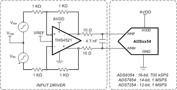
The ADS8354, ADS7854, and ADS7254 belong to a family of pin-compatible, dual, high-speed, simultaneous-sampling, analog-to-digital converters (ADCs) that support fully-differential analog inputs.
Each device includes two individually programmable reference sources that can be used for system-level gain calibration. Also, a flexible serial interface that can operate over a wide power-supply range enables easy communication with a large variety of host controllers. Power consumption for a given throughput can be optimized by using the two low-power modes supported by the device. All devices are fully specified over the extended industrial temperature range (–40°C to 125°C) and are available in pin-compatible, WQFN-16 (3-mm ×
3-mm) and TSSOP-16 packages.
Device Information(1)
| PART NUMBER | PACKAGE | BODY SIZE (NOM) |
|---|---|---|
| ADSxx54 | TSSOP (16) | 5.00 mm × 4.40 mm |
| WQFN (16) | 3.00 mm × 3.00 mm |
- For all available packages, see the orderable addendum at the end of the datasheet.
Typical Application Diagram