SBAS587A January 2014 – April 2014 ADS7251 , ADS7851
PRODUCTION DATA.
- 1 Features
- 2 Applications
- 3 Description
- 4 Revision History
- 5 Terminal Configuration and Functions
-
6 Specifications
- 6.1 Absolute Maximum Ratings
- 6.2 Handling Ratings
- 6.3 Recommended Operating Conditions
- 6.4 Thermal Information
- 6.5 Electrical Characteristics: ADS7251
- 6.6 Electrical Characteristics: ADS7851
- 6.7 Electrical Characteristics: Common
- 6.8 ADS7251 Timing Characteristics
- 6.9 ADS7851 Timing Characteristics
- 6.10 Typical Characteristics: ADS7251
- 6.11 Typical Characteristics: ADS7851
- 6.12 Typical Characteristics: Common
- 7 Detailed Description
- 8 Application and Implementation
- 9 Power Supply Recommendations
- 10Layout
- 11Device and Documentation Support
- 12Mechanical, Packaging, and Orderable Information
Package Options
Mechanical Data (Package|Pins)
- RTE|16
Thermal pad, mechanical data (Package|Pins)
- RTE|16
Orderable Information
1 Features
- 12- and 14-Bit Pin-Compatible Family
- Simultaneous Sampling of Two Channels
- Supports Fully-Differential Analog Inputs
- Independent Internal Reference (per ADC)
- High Speed:
- Up to 2 MSPS with the ADS7251 (12-Bit)
- Up to 1.5 MSPS with the ADS7851 (14-Bit)
- Excellent Performance:
- ADS7251:
- SNR: 73 dB
- INL: ±1 LSB
- ADS7851:
- SNR: 83.5 dB
- INL: ±2 LSB
- Fully-Specified Over the Extended Industrial Temperature Range: –40°C to +125°C
- Small Footprint: WQFN-16 (3 mm × 3 mm)
2 Applications
- Motor Control: Direct Interface to SinCos Encoders
- Optical Networking: EDFA Gain Control Loop
- Protection Relays
- Power Quality Measurement
- Three-Phase Power Controls
- Programmable Logic Controllers
- Industrial Automation
3 Description
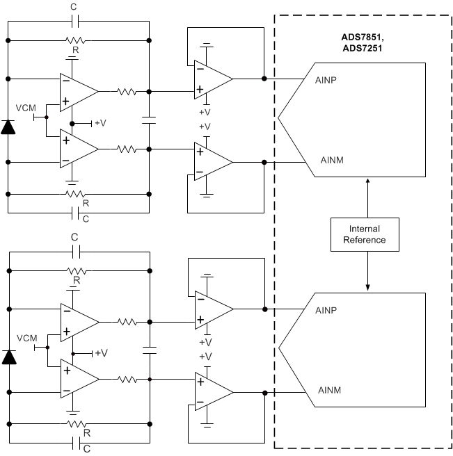
The ADS7251 and ADS7851 belong to a family of pin-compatible, dual, high-speed, simultaneous-sampling, analog-to-digital converters (ADCs) that support fully-differential analog inputs and feature two independent internal voltage references. The ADS7251 offers 12-bit resolution and up to 2-MSPS sampling speed. The ADS7851 offers 14-bit resolution and up to 1.5-MSPS sampling speed.
The devices support a wide digital supply voltage range, allowing easy communication with a variety of digital host controllers using a simple, serial interface. Both devices are fully specified over the extended industrial temperature range (–40°C to +125°C) and are available in a pin-compatible, space-saving, WQFN-16 (3-mm × 3-mm) package.
Device Information
| ORDER NUMBER | PACKAGE | BODY SIZE |
|---|---|---|
| ADS7251RTE | WQFN (16) | 3 mm × 3 mm |
| ADS7851RTE | WQFN (16) | 3 mm × 3 mm |
Typical Application Diagram