SBAS108E May 2000 – December 2016 ADS8320
PRODUCTION DATA.
- 1 Features
- 2 Applications
- 3 Description
- 4 Revision History
- 5 Pin Configuration and Functions
- 6 Specifications
- 7 Detailed Description
- 8 Application and Implementation
- 9 Power Supply Recommendations
- 10Layout
- 11Device and Documentation Support
- 12Mechanical, Packaging, and Orderable Information
Package Options
Mechanical Data (Package|Pins)
- DGK|8
Thermal pad, mechanical data (Package|Pins)
Orderable Information
1 Features
- 100-kHz Sampling Rate
-
microPower:
- 1.8 mW at 100 kHz and 2.7 V
- 0.3 mW at 10 kHz and 2.7 V
- Power Down: 3 µA (Maximum)
- 8-Pin VSSOP Package
- Pin-Compatible to ADS7816 and ADS7822
- Serial (SPI™/SSI) Interface
2 Applications
- Battery-Operated Systems
- Remote Data Acquisition
- Isolated Data Acquisition
- Simultaneous Sampling, Multichannel Systems
- Industrial Controls
- Robotics
- Vibration Analysis
3 Description
The ADS8320 device is a 16-bit, sampling analog-to-digital (A/D) converter with ensured specifications over a 2.7-V to 5.25-V supply range. It requires very little power even when operating at the full 100-kHz data rate. At lower data rates, the high speed of the device enables it to spend most of its time in the power-down mode. The average power dissipation is less than 100 mW at 10-kHz data rate.
The ADS8320 also features operation from 2 V to 5.25 V, a synchronous serial (SPI/SSI compatible) interface, and a differential input. The reference voltage can be set to any level within the range of 500 mV to VCC.
Ultra-low power and small size make the ADS8320 ideal for portable and battery-operated systems. It is also a perfect fit for remote data acquisition modules, simultaneous multi-channel systems, and isolated data acquisition. The ADS8320 is available in an
8-pin VSSOP package.
Device Information(1)
| PART NUMBER | PACKAGE | BODY SIZE (NOM) |
|---|---|---|
| ADS8320 | VSSOP (8) | 3.00 mm × 3.00 mm |
- For all available packages, see the orderable addendum at the end of the data sheet.
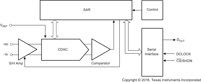
Block Diagram
