-
ADSxxx3 Dual, 1-MSPS, 16-, 14-, and 12-Bit, 4×2 or 2×2 Channel, Simultaneous Sampling Analog-to-Digital Converter
- 1 Features
- 2 Applications
- 3 Description
- 4 Revision History
- 5 Device Comparison Table
- 6 Pin Configuration and Functions
-
7 Specifications
- 7.1 Absolute Maximum Ratings
- 7.2 ESD Ratings
- 7.3 Recommended Operating Conditions
- 7.4 Thermal Information
- 7.5 Electrical Characteristics: General
- 7.6 Electrical Characteristics: ADS8363
- 7.7 Electrical Characteristics: ADS7263
- 7.8 Electrical Characteristics: ADS7223
- 7.9 Switching Characteristics
- 7.10 Typical Characteristics
- 8 Detailed Description
- 9 Application and Implementation
- 10Power Supply Recommendations
- 11Layout
- 12Device and Documentation Support
- 13Mechanical, Packaging, and Orderable Information
- IMPORTANT NOTICE
Package Options
Mechanical Data (Package|Pins)
- RHB|32
Thermal pad, mechanical data (Package|Pins)
- RHB|32
Orderable Information
ADSxxx3 Dual, 1-MSPS, 16-, 14-, and 12-Bit, 4×2 or 2×2 Channel, Simultaneous Sampling Analog-to-Digital Converter
1 Features
- Eight Pseudo- or Four Fully-Differential Inputs
- Simultaneous Sampling of Two Channels
- Excellent AC Performance:
- SNR:
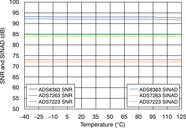
93 dB (ADS8363)
85 dB (ADS7263)
73 dB (ADS7223) - THD:
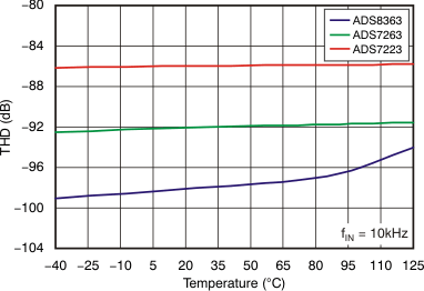
–98 dB (ADS8363)
–92 dB (ADS7263)
–86 dB (ADS7223)
- SNR:
- Dual Programmable and Buffered 2.5-V Reference Allows:
- Two Different Input Voltage Range Settings
- Two-Level PGA Implementation
- Programmable Auto-Sequencer
- Integrated Data Storage (up to 4 per channel) for Oversampling Applications
- 2-Bit Counter for Safety Applications
- Fully Specified Over the Extended Industrial Temperature Range: –40°C to +125°C
2 Applications
- Motor Control: Current and Position Measurement including Safety Applications
- Power Quality Measurement
- Three-Phase Power Control
- Programmable Logic Controllers
- Industrial Automation
- Protection Relays
3 Description
The ADS8363 is a dual, 16-bit, 1-MSPS analog-to-digital converter (ADC) with eight pseudo- or four fully-differential input channels grouped into two pairs for simultaneous signal acquisition. The analog inputs are maintained differentially to the input of the ADC. The input multiplexer can be used in either pseudo-differential mode, supporting up to four channels per ADC (4x2), or in fully-differential mode that allows to convert up to two inputs per ADC (2x2). The ADS7263 is a 14-bit version and the ADS7223 is a 12-bit version of the ADS8363.
The ADS8363, ADS7263, and ADS7223 offer two programmable reference outputs, flexible supply voltage ranges, a programmable auto-sequencer, data storage of up to four conversion results per channel, and several power-down features.
All devices are offered in a 5-mm x 5-mm, 32-pin VQFN package.
Device Information(1)
| PART NUMBER | PACKAGE | BODY SIZE (NOM) |
|---|---|---|
| ADSxxx3 | VQFN (32) | 5.00 mm x 5.00 mm |
- For all available packages, see the package option addendum at the end of the data sheet.
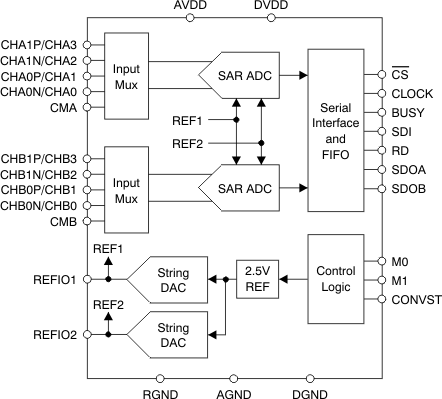
Functional Block Diagram
4 Revision History
Changes from C Revision (January 2017) to D Revision
- Changed operating temperature from 85°C to 125°C in Recommended Operating Conditions tableGo
Changes from B Revision (January 2011) to C Revision
- Added Device Information table, ESD Ratings table, Recommended Operating Conditions table, Feature Description section, Device Functional Modes section, Application and Implementation section, Power Supply Recommendations section, Layout section, Device and Documentation Support section, and Mechanical, Packaging, and Orderable Information sectionGo
- Changed ADS8363/7263/7223 to ADS8363, ADS7263, and ADS7223 throughout documentGo
- Changed Description section: changed last sentence of first paragraph and last paragraph Go
- Changed Device Comparison Table titleGo
- Changed Pin Configuration and Functions section titleGo
- Changed footnote of Figure 1 and 1 for clarityGo
- Changed second and third columns of Midscale – 1 LSB row in Output Data Format table: changed –VREF to –2VREF in column 2, changed last two voltage values in column 3Go
- Changed footnote of Figure 31 Go
- Changed footnote of Figure 32 Go
- Changed footnote of Figure 33 Go
- Changed footnote of Figure 34 Go
- Changed footnote of Figure 35 Go
- Changed footnote of Figure 36 Go
- Changed footnote of Figure 38 Go
- Changed footnote of Figure 40 Go
- Changed 1FFh to 3FFh in bits 9-0 description of REFDAC1 Control Register and REFDAC2 Control RegisterGo
Changes from A Revision (December, 2010) to B Revision
- Revised test conditions for gain error parameterGo
- Revised test conditions for gain error parameterGo
- Revised test conditions for gain error parameterGo
- Updated CONVST high time specificationGo
- Revised CONVST sectionGo
- Revised Mode II sectionGo
- Revised Special Read Mode II sectionGo
- Revised Fully-Differential Mode IV sectionGo
- Revised Special Mode IV sectionGo
- Added CONVST section in ADS8361 CompatibilityGo
Changes from * Revision (October, 2010) to A Revision
5 Device Comparison Table
| PRODUCT | RESOLUTION | NMC | INL | SNR | THD |
|---|---|---|---|---|---|
| ADS8363 | 16 bits | 16 or 15 bits(1) | ±3 or ±4 LSB(1) | 93 dB (typ) | –98 dB (typ) |
| ADS7263 | 14 bits | 14 bits | ±1 LSB | 85 dB (typ) | –92 dB (typ) |
| ADS7223 | 12 bits | 12 bits | ±0.5 LSB | 73 dB (typ) | –86 dB (typ) |
6 Pin Configuration and Functions
Pin Functions
| PIN | TYPE(1) | DESCRIPTION | |
|---|---|---|---|
| NAME | NO. | ||
| AGND | 12, 30 | P | Analog ground. Connect to analog ground plane. |
| AVDD | 13, 29 | P | Analog power supply, 2.7 V to 5.5 V. Decouple to AGND with a 1-μF ceramic capacitor. |
| BUSY | 23 | DO | Converter busy indicator. BUSY goes high when the inputs are in hold mode and returns to low after the conversion is complete. |
| CHA0N/CHA0 | 8 | AI | Fully-differential inverting analog input channel A1 or pseudo-differential input A0 |
| CHA0P/CHA1 | 7 | AI | Fully-differential noninverting analog input channel A1 or pseudo-differential input A1 |
| CHA1N/CHA2 | 6 | AI | Fully-differential inverting analog input channel A1 or pseudo-differential input A2 |
| CHA1P/CHA3 | 5 | AI | Fully-differential noninverting analog input channel A1 or pseudo-differential input A3 |
| CHB0N/CHB0 | 4 | AI | Fully-differential inverting analog input channel B0 or pseudo-differential input B0 |
| CHB0P/CHB1 | 3 | AI | Fully-differential noninverting analog input channel B0 or pseudo-differential input B1 |
| CHB1N/CHB2 | 2 | AI | Fully-differential inverting analog input channel B1 or pseudo-differential input B2 |
| CHB1P/CHB3 | 1 | AI | Fully-differential noninverting analog input channel B1 or pseudo-differential input B3 |
| CLOCK | 22 | DI | External clock input. The range is 0.5 MHz to 20 MHz in half-clock mode, or 1 MHz to 40 MHz in full-clock mode. |
| CMA | 31 | AI | Common-mode voltage input for channels Ax (in pseudo-differential mode only). |
| CMB | 32 | AI | Common-mode voltage input for channels Bx (in pseudo-differential mode only). |
| CONVST | 19 | DI | Conversion start. The ADC switches from sample into hold mode on the rising edge of CONVST. Thereafter, the conversion starts with the next rising edge of the CLOCK pin. |
| CS | 21 | DI | Chip select. When this pin is low, the SDOx, SDI, and RD pins are active; when this pin is high, the SDOx outputs are 3-stated, and the SDI and RD inputs are ignored. |
| DGND | 28 | P | Digital ground. Connect to digital ground plane. |
| DVDD | 27 | P | Digital supply, 2.3 V to 5.5 V. Decouple to DGND with a 1-μF ceramic capacitor. |
| M0 | 17 | DI | Mode pin 0. Selects analog input channel mode (see Table 5). |
| M1 | 16 | DI | Mode pin 1. Selects the digital output mode (see Table 5). |
| NC | 14, 15, 26 | NC | This pin is not internally connected. |
| RD | 20 | DI | Read data. Synchronization pulse for the SDOx outputs and SDI input. RD only triggers when CS is low. |
| REFIO1 | 9 | AIO | Reference voltage input/output 1. A ceramic capacitor of 22 µF connected to RGND is required. |
| REFIO2 | 10 | AIO | Reference voltage input/output 2. A ceramic capacitor of 22 µF connected to RGND is required. |
| RGND | 11 | P | Reference ground. Connect to analog ground plane with a dedicated via. |
| SDI | 18 | DI | Serial data input. This pin is used to set up of the internal registers, and can also be used in ADS8361-compatible manner. The data on SDI are ignored when CS is high. |
| SDOA | 25 | DO | Serial data output for converter A. 3-state when CS is high. |
| SDOB | 24 | DO | Serial data output for converter B. Active only if M1 is low. 3-state when CS is high. |
7 Specifications
7.1 Absolute Maximum Ratings
over operating free-air temperature range (unless otherwise noted)(1)| MIN | MAX | UNIT | ||
|---|---|---|---|---|
| Supply voltage, AVDD to AGND or DVDD to DGND | –0.3 | 6 | V | |
| Supply voltage, DVDD to AVDD | 1.2 × AVDD(2) | V | ||
| Analog and reference input voltage with respect to AGND | AGND – 0.3 | AVDD + 0.3 | V | |
| Digital input voltage with respect to DGND | DGND – 0.3 | DVDD + 0.3 | V | |
| Ground voltage difference |AGND-DGND| | 0.3 | V | ||
| Input current to any pin except supply pins | –10 | 10 | mA | |
| Maximum virtual junction temperature, TJ | 150 | °C | ||
| Storage temperature, Tstg | –65 | 150 | °C | |
7.2 ESD Ratings
| VALUE | UNIT | |||
|---|---|---|---|---|
| V(ESD) | Electrostatic discharge | Human-body model (HBM), per ANSI/ESDA/JEDEC JS-001(1) | ±2000 | V |
| Charged-device model (CDM), per JEDEC specification JESD22-C101(2) | ±500 | |||
7.3 Recommended Operating Conditions
over operating free-air temperature range (unless otherwise noted)| MIN | NOM | MAX | UNIT | ||
|---|---|---|---|---|---|
| AVDD | Analog supply voltage | 5 | V | ||
| DVDD | Digital supply voltage | 3.3 | V | ||
| Operating temperature | –40 | 125 | °C | ||
7.4 Thermal Information
| THERMAL METRIC(1) | ADS8363, ADS7263, ADS7223 | UNIT | |
|---|---|---|---|
| RHB (VQFN) | |||
| 32 PINS | |||
| RθJA | Junction-to-ambient thermal resistance | 33.3 | °C/W |
| RθJC(top) | Junction-to-case (top) thermal resistance | 29.5 | °C/W |
| RθJB | Junction-to-board thermal resistance | 7.3 | °C/W |
| ψJT | Junction-to-top characterization parameter | 0.2 | °C/W |
| ψJB | Junction-to-board characterization parameter | 7.4 | °C/W |
| RθJC(bot) | Junction-to-case (bottom) thermal resistance | 0.9 | °C/W |
7.5 Electrical Characteristics: General
All minimum and maximum specifications at TA = –40°C to +125°C, specified supply voltage range, VREF = 2.5 V (int), and tDATA = 1 MSPS (unless otherwise noted). Typical values are at TA = +25°C, AVDD = 5 V, and DVDD = 3.3 V.| PARAMETER | TEST CONDITIONS | MIN | TYP | MAX | UNIT | |
|---|---|---|---|---|---|---|
| ANALOG INPUT | ||||||
| FSR | Full-scale input range | (CHxxP – CHxxN) or CHxx to CMx | –VREF | +VREF | V | |
| VIN | Absolute input voltage | CHxxx to AGND | –0.1 | AVDD + 0.1 | V | |
| CIN | Input capacitance | CHxxx to AGND | 45 | pF | ||
| CID | Differential input capacitance | 22.5 | pF | |||
| IIL | Input leakage current | –16 | 16 | nA | ||
| PSRR | Power-supply rejection ratio | AVDD = 5.5 V | 75 | dB | ||
| SAMPLING DYNAMICS | ||||||
| tCONV | Conversion time per ADC | Half-clock mode | 17.5 | tCLK | ||
| Full-clock mode | 35 | |||||
| tACQ | Acquisition time | Half-clock mode | 2 | tCLK | ||
| Full-clock Mode | 4 | |||||
| fDATA | Data rate | 25 | 1000 | kSPS | ||
| tA | Aperture delay | 6 | ns | |||
| tA match | ADC to ADC | 50 | ps | |||
| tAJIT | Aperture jitter | 50 | ps | |||
| fCLK | Clock frequency | Half-clock mode | 0.5 | 20 | MHz | |
| Full-clock mode | 1 | 40 | ||||
| tCLK | Clock period | Half-clock mode | 50 | 2000 | ns | |
| Full-clock mode | 25 | 1000 | ||||
| INTERNAL VOLTAGE REFERENCE | ||||||
| Resolution | Reference output DAC resolution | 10 | Bits | |||
| VREFOUT | Reference output voltage | Over 20% to 100% DAC range | 0.2VREFOUT | VREFOUT | V | |
| REFIO1, DAC = 3FFh | 2.485 | 2.500 | 2.515 | |||
| REFIO2, DAC = 3FFh | 2.480 | 2.500 | 2.520 | |||
| dVREFOUT/dT | Reference voltage drift | ±10 | ppm/°C | |||
| DNLDAC | DAC differential linearity error | –4 | ±1 | 4 | LSB | |
| INLDAC | DAC integral linearity error | –4 | ±0.5 | 4 | LSB | |
| VOSDAC | DAC offset error | VREFOUT = 0.5 V | –4 | ±1 | 4 | LSB |
| PSRR | Power-supply rejection ratio | 73 | dB | |||
| IREFOUT | Reference output dc current | –2 | +2 | mA | ||
| IREFSC | Reference output short-circuit current(1) | 50 | mA | |||
| tREFON | Reference output settling time | CREF = 22 μF | 8 | ms | ||
| VOLTAGE REFERENCE INPUT | ||||||
| VREF | Reference input voltage range | 0.5 | 2.5 | 2.525 | V | |
| IREF | Reference input current | 50 | μA | |||
| CREF | External ceramic reference capacitance | 22 | μF | |||
| DIGITAL INPUTS(2) | ||||||
| IIN | Input current | VIN = DVDD to DGND | –50 | +50 | nA | |
| CIN | Input capacitance | 5 | pF | |||
| Logic family | CMOS with Schmitt-Trigger | |||||
| VIH | High-level input voltage | DVDD = 4.5 V to 5.5 V | 0.7DVDD | DVDD + 0.3 | V | |
| VIL | Low-level input voltage | DVDD = 4.5 V to 5.5 V | –0.3 | 0.3DVDD | V | |
| Logic family | LVCMOS | |||||
| VIH | High-level input voltage | DVDD = 2.3 V to 3.6 V | 2 | DVDD + 0.3 | V | |
| VIL | Low-level input voltage | DVDD = 2.3 V to 3.6 V | –0.3 | 0.8 | V | |
| DIGITAL OUTPUTS(2) | ||||||
| COUT | Output capacitance | 5 | pF | |||
| CLOAD | Load capacitance | 30 | pF | |||
| Logic family | CMOS | |||||
| VOH | High-level output voltage | DVDD = 4.5 V, IOH = –100 µA | 4.44 | V | ||
| VOL | Low-level output voltage | DVDD = 4.5 V, IOH = +100 µA | 0.5 | V | ||
| Logic family | LVCMOS | |||||
| VOH | High-level output voltage | DVDD = 2.3 V, IOH = –100 µA | DVDD – 0.2 | V | ||
| VOL | Low-level output voltage | DVDD = 2.3 V, IOH = +100 µA | 0.2 | V | ||
| POWER SUPPLY | ||||||
| AVDD | Analog supply voltage | AVDD to AGND, half-clock mode | 2.7 | 5.0 | 5.5 | V |
| AVDD to AGND, full-clock mode | 4.5 | 5.0 | 5.5 | |||
| DVDD | Digital supply voltage | 3-V and 3.3-V levels | 2.3 | 2.5 | 3.6 | V |
| 5-V levels, half-clock mode only | 4.5 | 5.0 | 5.5 | |||
| AIDD | Analog supply current | AVDD = 3.6 V | 12.0 | 16.0 | mA | |
| AVDD = 5.5 V | 15.0 | 20.0 | ||||
| AVDD = 3.6 V, sleep and auto-sleep modes | 0.8 | 1.2 | ||||
| AVDD = 5.5 V, sleep and auto-sleep modes | 0.9 | 1.4 | ||||
| Power-down mode | 0.005 | |||||
| DIDD | Digital supply current | DVDD = 3.6 V, CLOAD = 10 pF | 1.1 | 2.5 | mA | |
| DVDD = 5.5 V, CLOAD = 10 pF | 3 | 6 | ||||
| PD | Power dissipation (normal operation) | AVDD = DVDD = 3.6 V | 47.2 | 66.6 | mW | |
| AVDD = 5.5 V, DVDD = 3.6 V | 86.5 | 117.0 | ||||
7.6 Electrical Characteristics: ADS8363
All minimum and maximum specifications at TA = –40°C to +125°C, specified supply voltage range, VREF = 2.5 V (int), and tDATA = 1 MSPS (unless otherwise noted). Typical values are at TA = +25°C, AVDD = 5 V, and DVDD = 3.3 V.7.7 Electrical Characteristics: ADS7263
All minimum and maximum specifications at TA = –40°C to +125°C, specified supply voltage range, VREF = 2.5 V (int), and tDATA = 1 MSPS (unless otherwise noted). Typical values are at TA = +25°C, AVDD = 5 V, and DVDD = 3.3 V.7.8 Electrical Characteristics: ADS7223
All minimum and maximum specifications at TA = –40°C to +125°C, specified supply voltage range, VREF = 2.5 V (int), and tDATA = 1 MSPS (unless otherwise noted). Typical values are at TA = +25°C, AVDD = 5 V, and DVDD = 3.3 V.7.9 Switching Characteristics(1)
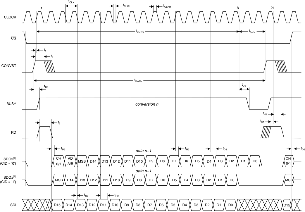
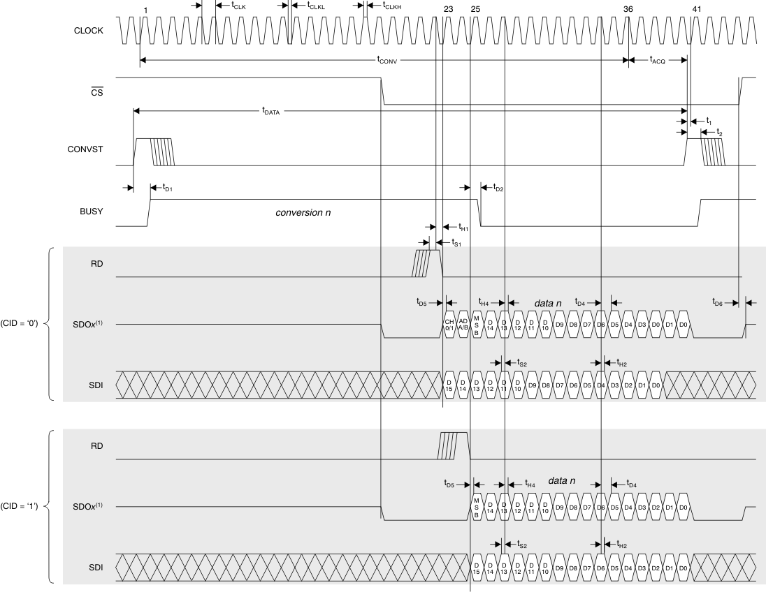
Over the recommended operating free-air temperature range of –40°C to +125°C, and DVDD = 2.3 V to 5.5 V (unless otherwise noted).| MIN | MAX | UNIT | |||
|---|---|---|---|---|---|
| tDATA | Data throughput, fCLK = max | 1 | μs | ||
| tCONV | Conversion time | Half-clock mode | 17.5 | tCLK | |
| Full-clock mode | 35 | ||||
| tACQ | Acquisition time | 100 | ns | ||
| fCLK | CLOCK frequency | Half-clock mode | 0.5 | 20 | MHz |
| Full-clock mode | 1 | 40 | |||
| tCLK | CLOCK period | Half-clock mode | 50 | 2000 | ns |
| Full-clock mode | 25 | 1000 | |||
| tCLKL | CLOCK low time | 11.25 | ns | ||
| tCLKH | CLOCK high time | 11.25 | ns | ||
| t1 | CONVST rising edge to first CLOCK rising edge | 12 | ns | ||
| t2 | CONVST high time | 10 | ns | ||
| Half-clock mode: timing modes II and IV only | 1 | tCLK | |||
| t3 | RD high time, half-clock mode: timing modes II, IV, SII, and SIV only | 1 | tCLK | ||
| tS1 | RD high to CLOCK falling edge setup time | 5 | ns | ||
| tH1 | RD high to CLOCK falling edge hold time | 5 | ns | ||
| tS2 | Input data to CLOCK falling edge setup time | 5 | ns | ||
| tH2 | Input data to CLOCK falling edge hold time | 4 | ns | ||
| tD1 | CONVST rising edge to BUSY high delay(2) | 2.3 V < DVDD < 3.6 V | 19 | ns | |
| 4.5 V < DVDD < 5.5 V | 16 | ||||
| tD2 | CLOCK 18th falling edge (half-clock mode) or 24th rising edge (full-clock mode) to BUSY low delay | 2.3 V < DVDD < 3.6 V | 25 | ns | |
| 4.5 V < DVDD < 5.5 V | 20 | ||||
| tD3 | CLOCK rising edge to next data valid delay | Half-clock mode, 2.3 V < DVDD < 3.6 V |
14 | ns | |
| Half-clock mode, 4.5 V < DVDD < 5.5 V |
12 | ||||
| tH3 | Output data to CLOCK rising edge hold time, half-clock mode | 3 | ns | ||
| tD4 | CLOCK falling edge to next data valid delay, full-clock mode | 19 | ns | ||
| tH4 | Output data to CLOCK falling edge hold time, full-clock mode | 7 | ns | ||
| tD5 | RD falling edge to first data valid | 2.3 V < DVDD < 3.6 V | 16 | ns | |
| 4.5 V < DVDD < 5.5 V | 12 | ||||
| tD6 | CS rising edge to SDOx 3-state | 6 | ns | ||
7.10 Typical Characteristics
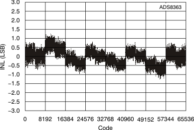
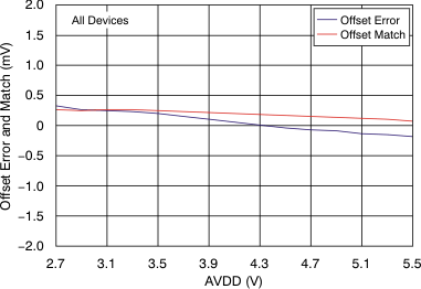
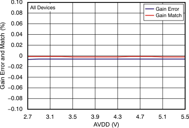
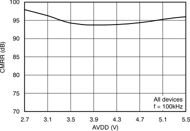
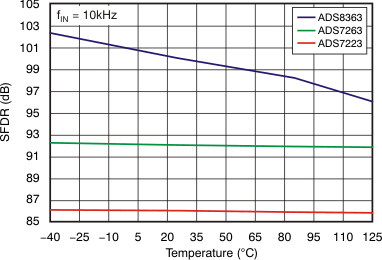
at TA = +25°C, AVDD = 5 V, DVDD = 3.3 V, VREF = 2.5 V (internal), and fDATA = 1 MSPS (unless otherwise noted)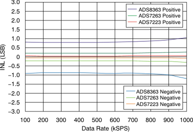
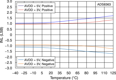
Analog Supply Voltage
Analog Supply Voltage
Analog Supply Voltage
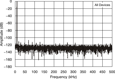
(4096 Point FFT; fIN = 10 kHz)
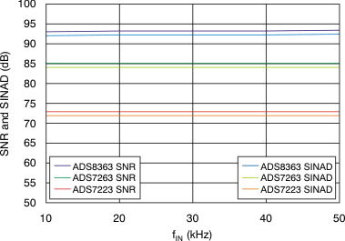
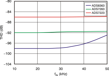
Input Signal Frequency
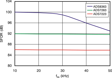
Input Signal Frequency
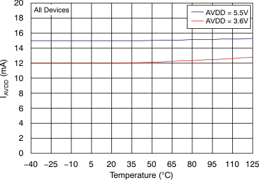
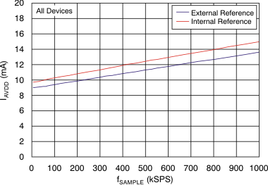
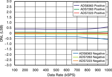
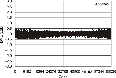
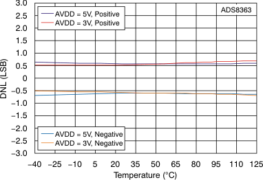
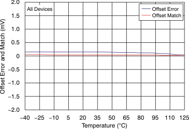
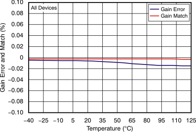
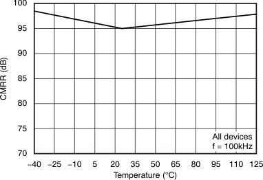
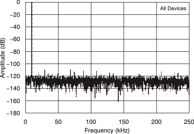
(4096 Point FFT; fIN = 10 kHz, fSAMPLE = 0.5 MSPS)
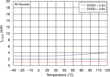
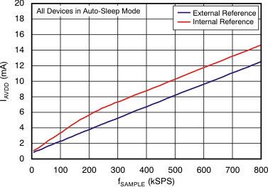
(Auto-Sleep Mode)
8 Detailed Description
8.1 Overview
The ADS8363, ADS7263, and ADS7223 contain two 16-, 14-, and 12-bit analog-to-digital converters (ADCs), respectively, that operate based on the successive approximation register (SAR) principle. These ADCs sample and convert simultaneously. Conversion time can be as low as 875 ns. Adding an acquisition time of 100 ns, and a margin of 25 ns for propagation delay and CONVST pulse generation, results in a maximum conversion rate of 1 MSPS.
Each ADC has a fully-differential 2:1 multiplexer front-end. In many common applications, all negative input signals remain at the same constant voltage (for example, 2.5 V). For these applications, the multiplexer can be used in a pseudo-differential 4:1 mode, where the CMx pins function as common-mode pins and all four analog inputs are referred to the corresponding CMx pin.
The ADS8363, ADS7263, and ADS7223 also include a 2.5-V internal reference. This reference drives two independently-programmable, 10-bit digital-to-analog converters (DACs), allowing the voltage at each of the REFIOx pins to be adjusted through the internal REFDACx registers in 2.44-mV steps. A low-noise, unity-gain operational amplifier buffers each of the DAC outputs and drives the REFIOx pin.
The ADS8363, ADS7263, and ADS7223 provide a serial interface that is compatible with the ADS8361. However, instead of the ADS8361 A0 pin that controls the channel selection, the ADS8363, ADS7263, and ADS7223 offers a serial data input (SDI) pin that supports additional functions described in the Digital section of this data sheet (also see the section).
8.2 Functional Block Diagram

8.3 Feature Description
8.3.1 Analog
This section discusses the analog input circuit, the ADCs, and the reference design of the device.
8.3.1.1 Analog Inputs
Each ADC is fed by an input multiplexer, as shown in Figure 27. Each multiplexer is used in either a fully-differential 2:1 configuration (as shown in Table 1) or a pseudo-differential 4:1 configuration (as shown in Table 2).
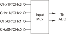 Figure 27. Input Multiplexer Configuration
Channel selection is performed using either the external M0 pin or the C[1:0] bits in the Configuration (CONFIG) register in fully-differential mode, or using the SEQFIFO register in pseudo-differential mode. In either case, changing the multiplexer settings impacts the conversion started with the next CONVST pulse.
Table 1. Fully-Differential 2:1 Multiplexer Configuration
| C1 | C0 | ADC+ | ADC– |
|---|---|---|---|
| 0 | x | CHx0P | CHx0N |
| 1 | x | CHx1P | CHx1N |
Table 2. Pseudo-Differential 4:1 Multiplexer Configuration
| C1 | C0 | ADC+ | ADC– |
|---|---|---|---|
| 0 | 0 | CHx0 | CMx/REFIOx |
| 0 | 1 | CHx1 | CMx/REFIOx |
| 1 | 0 | CHx2 | CMx/REFIOx |
| 1 | 1 | CHx3 | CMx/REFIOx |
The input path for the converter is fully differential and provides a good common-mode rejection of 92 dB at 100 kHz (for the ADS8363). The high CMRR also helps suppress noise in harsh industrial environments.
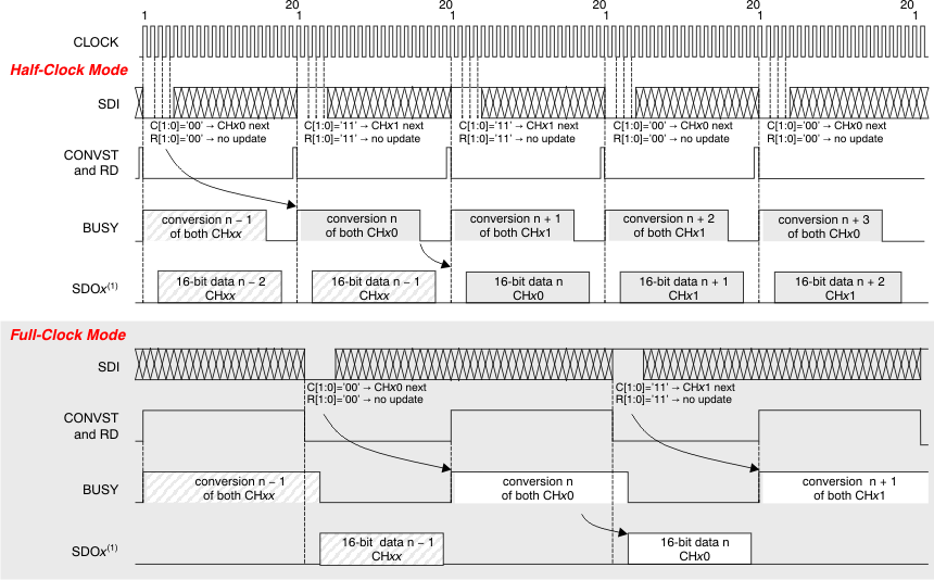
Each of the 40-pF sample-and-hold capacitors (CS in Figure 28) is connected through switches to the multiplexer output. Opening the switches holds the sampled data during the conversion process. After the conversion completes, both capacitors are precharged for the duration of one clock cycle to the voltage present at the REFIOx pin. After precharging, the multiplexer outputs are connected to the sampling capacitors again. The voltage at the analog input pin is usually different from the reference voltage; therefore, the sample capacitors must be charged to within one-half LSB for 16-, 14-, or 12-bit accuracy during the acquisition time tACQ (see Figure 1 and Figure 2).
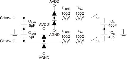 Figure 28. Equivalent Analog Input Circuit
Acquisition is indicated with the BUSY signal being low. Acquisition starts by closing the input switches (after finishing the previous conversion and precharging) and finishes with the rising edge of the CONVST signal. If the device operates at full speed, the acquisition time is typically 100 ns.
The minimum –3-dB bandwidth of the driving operational amplifier can be calculated as shown in Equation 1, with n = 16 for the resolution of the ADS8363, n = 14 for the ADS7263, or n = 12 for the ADS7223:

With tACQ = 100 ns, the minimum bandwidth of the driving amplifier is 19 MHz for the ADS8363, 17 MHz for the ADS7263, and 15 MHz for the ADS7223. The required bandwidth can be lower if the application allows a longer acquisition time.
A gain error occurs if a given application does not fulfill the settling requirement shown in Equation 1. However, linearity and THD are not directly affected as a result of precharging the capacitors.
The OPA365 from Texas Instruments is recommended as a driver; in addition to offering the required bandwidth, the OPA365 also provides a low offset and excellent THD performance (see the Application and Implementation section).
The phase margin of the driving operational amplifier is usually reduced by the ADC sampling capacitor. A resistor placed between the capacitor and the amplifier limits this effect; therefore, an internal 100-Ω resistor (RSER) is placed in series with the switch. The switch resistance (RSW) is typically 100 Ω; see Figure 28).
An input driver may not be required, if the impedance of the signal source (RSOURCE) fulfills the requirement of Equation 2:

where
- n = 16, 14, 12 for the resolution of the ADS8363, ADS7263, and ADS7223, respectively
- CS = 40-pF sample capacitance
- RSER = 100-Ω input resistor value
- RSW = 100-Ω switch resistance value
With tACQ = 100 ns, the maximum source impedance must be less than 12 Ω for the ADS8363, less than 40 Ω for the ADS7263, and less than 77 Ω for the ADS7223. The source impedance can be higher if the ADC is used at a lower data rate.
The differential input voltage range of the ADC is ±VREF, the voltage at the selected REFIOx pin.
The voltage to all inputs must be kept within the 0.3-V limit below AGND and above AVDD, without allowing dc current to flow through the inputs (exceeding these limits causes the internal ESD diodes to conduct, leading to increased leakage current that may damage the device). Current is only necessary to recharge the sample-and-hold capacitors.
Unused inputs must be directly tied to AGND or RGND without the need of a pull-down resistor.
8.3.1.2 Analog-to-Digital Converters (ADCs)
The ADS8363, ADS7263, and ADS7223 include two SAR-type, 1 MSPS, 16-, 14-, and 12-bit ADCs that include sample-and-hold, respectively; see the Functional Block Diagram section.
8.3.1.3 CONVST
The analog inputs are held with the rising edge of the CONVST (conversion start) signal. The setup time of CONVST referred to the next rising edge of CLOCK (system clock) is 12 ns (minimum). The conversion automatically starts with the rising CLOCK edge. Do not issue a rising edge of CONVST during a conversion (that is, when BUSY is high).
RD (read data) and CONVST can be shorted to minimize necessary software and wiring. The RD signal is triggered by the device on the falling edge of CLOCK. Therefore, the combined signals must be activated with the rising CLOCK edge. The conversion then starts with the subsequent rising CLOCK edge. In modes with only SDOA active (that is, in modes II, IV, SII, and SIV), the maximum length of the combined RD and CONVST signal is one clock cycle if the half-clock timing is used.
If CONVST and RD are combined, CS must be low whenever a new conversion starts; however, this condition is not required if RD and CONVST are controlled separately. Note that if FIFO is used, CONVST must be controlled separately from RD.
After completing a conversion, the sample capacitors are automatically precharged to the value of the reference voltage used to significantly reduce the crosstalk among the multiplexed input channels.
8.3.1.4 CLOCK
The ADS8363, ADS7263, and ADS7223 use an external clock with an allowable frequency range that depends on the mode being used. By default (after power-up), the ADC operates in half-clock mode that supports a clock in the range of 0.5 MHz to 20 MHz. In full-clock mode, the ADC requires a clock in the range of 1 MHz to 40 MHz. For maximum data throughput, the clock signal must be continuously running. However, in applications that use the device in burst mode, the clock can be held static low or high upon completion of the read access and before starting a new conversion.
The CLOCK duty cycle must be 50%. However, the device functions properly with a duty cycle between 30% and 70%.
8.3.1.5 RESET
The ADS8363, ADS7263, and ADS7223 feature an internal power-on reset (POR) function. A user-controlled reset can also be issued using SDI register bits A[3:0] (see the Digital section).
8.3.1.6 REFIOx
The ADS8363, ADS7263, and ADS7223 include a low-drift, 2.5-V internal reference source. This source feeds two, 10-bit string DACs that are controlled through registers. As a result of this architecture, the reference voltages at REFIOx are programmable in 2.44-mV steps and can be adjusted to the application requirements without the use of additional external components. The actual output voltage can be calculated using Equation 3, with code being the decimal value of the REFDACx register content:

The reference DAC has a fixed transition at the code 508 (0x1FC). At this code, the DAC can show a jump of up to 10 mV in the transfer function. Table 3 lists some examples of internal reference DAC settings. However, to ensure proper performance, the REFDACx output voltage must not be programmed below 0.5 V.
Table 3. REFDACx Setting Examples
| VREFOUT (NOM) | DECIMAL CODE | BINARY CODE | HEXADECIMAL CODE |
|---|---|---|---|
| 0.5000 V | 205 | 00 1100 1101 | 0CDh |
| 1.2429 V | 507 | 01 1111 1100 | 1FBh |
| 1.2427 V | 508 | 01 1111 1101 | 1FCh |
| 2.5000 V | 1023 | 11 1111 1111 | 3FFh |
A minimum of 22-μF capacitance is required on each REFIOx output to keep the references stable. The settling time is 8 ms (maximum) with the reference capacitor connected. Smaller reference capacitance values reduce the DNL, INL, and ac performance of the device. By default, both reference outputs are disabled and the respective values are set to 2.5 V after power-up.
For applications that use an external reference source, the internal reference can be disabled (default) using the RPD bit in the CONFIG register (see the Digital section). The REFIOx pins are directly connected to the ADC; therefore, the internal switching generates spikes that can be observed at this pin. Therefore, also in this case, an external 22-µF capacitor to the analog ground (AGND) must be used to stabilize the reference input voltage.
Disabled REFIOx pins can be left floating or can be directly tied to AGND or RGND.
Each of the reference DAC outputs can be individually selected as a source for each channel input using the Rxx bits in the REFCM register. Figure 29 shows a simplified block diagram of the internal circuit.
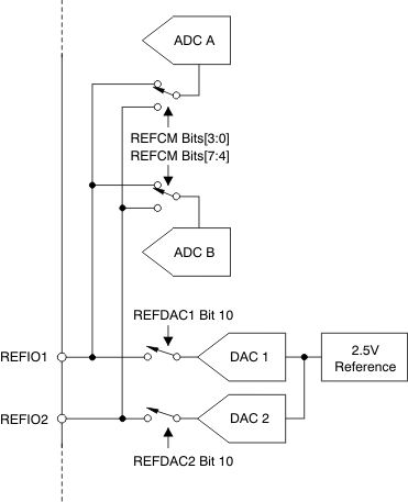 Figure 29. Reference Selection Circuit
8.3.2 Digital
This section reviews the timing and control of the serial interface.
The ADS8363, ADS7263, and ADS7223 offer a set of internal registers (see the Register Maps section for details) that allows the control of several features and modes of the device, as Table 4 shows.
Table 4. Supported Operating Modes
| INPUT SIGNAL TYPE | MANUAL CHANNEL SELECTION | AUTOMATIC CHANNEL SELECTION |
|---|---|---|
| Fully-differential (PDE bit = '0') |
Operating modes: I, II, and special mode II Channel information selectable through CID bit FIFO: not available |
Operating modes: III, IV and special mode IV Channel information selectable through CID bit FIFO: available in mode III and special mode IV; when used, a single read pulse allows reading of all data |
| Pseudo-differential (PDE bit = '1') |
Operating modes: I, II and special mode II Channel information selectable through CID bit FIFO: not available |
Operating modes: III and special mode IV Channel information not available (CID bit forced to '1') FIFO: available in mode III and special mode IV; when used, a single read pulse allows reading of all data Pseudo-differential sequencer is enabled |
8.3.2.1 Mode Selection Pin M0 and M1
The ADS8363, ADS7263, and ADS7223 can be configured to four different operating modes by using mode pins M0 and M1, as shown in Table 5.
Table 5. M0, M1 Truth Table
| M0 | M1 | CHANNEL SELECTION | SDOx USED |
|---|---|---|---|
| 0 | 0 | Manual (through SDI) | SDOA and SDOB |
| 0 | 1 | Manual (through SDI) | SDOA only |
| 1 | 0 | Automatic | SDOA and SDOB |
| 1 | 1 | Automatic | SDOA only |
The M0 pin sets either manual or automatic channel selection. In Manual mode, CONFIG register bits C[1:0] are used to select between channels CHx0 and CHx1. In Automatic mode, CONFIG register bits C[1:0] are ignored and channel selection is controlled by the device after each conversion. The automatic channel selection is only performed on fully-differential inputs in this case; for pseudo-differential inputs, the internal sequencer controls the input multiplexer.
The M1 pin selects between serial data being transmitted simultaneously on both SDOA and SDOB outputs for each channel, respectively, or using only the SDOA output for transmitting data from both channels (see Figure 31 through Figure 36 and the associated text for more information).
Additionally, the SDI pin is used for controlling device functionality through the internal register; see the Register Maps section for details.
8.3.2.2 Half-Clock Mode (Default Mode After Power-Up and Reset)
The ADS8363, ADS7263, and ADS7223 power up in half-clock mode, in which the ADC requires at least 20 CLOCKs for a complete conversion cycle, including the acquisition phase. The conversion result can only be read during the next conversion cycle. The first output bit is available with the falling RD edge, and the following output data bits are refreshed with the rising edge of CLOCK.
8.3.2.3 Full-Clock Mode (Allowing Conversion and Data Readout Within 1 µs, Supported In Dual Output Modes)
The full-clock mode allows converting data and reading the result within 1µ s. The entire cycle requires 40 CLOCKs. The first output bit is available with the falling RD edge and the following output data bits are refreshed with the falling edge of the CLOCK in this mode.
The full-clock mode can only be used with analog power supply AVDD in the range of 4.5 V to 5.5 V and digital supply DVDD in the range of 2.3 V to 3.6 V. The internal FIFO is disabled in full-clock mode.
8.3.2.4 2-Bit Counter
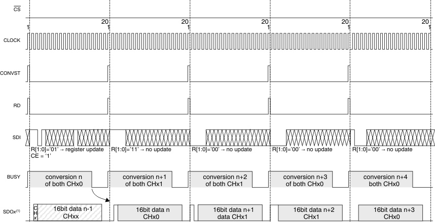
These devices offers a selectable 2-bit counter (activated using the CE bit in the CONFIG register) that is a useful feature in safety applications. The counter value automatically increments whenever a new conversion result is stored in the output register, indicating a new value. The counter default value after power-up is '01' (followed by '10', '11', '00', '01', and so on); see Figure 40. Because the counter value increments only when a new conversion results are transferred to the output register, this counter is used to verify that the ADC has performed a conversion and the data read is the result of this new conversion (not a old result read multiple times).
8.4 Device Functional Modes
8.4.1 Power-Down Modes and Reset
These devices have a comprehensive built-in power-down feature. There are three power-down modes: Power-Down, Sleep, and Auto-Sleep Power-Down. All three power-down modes are activated with the completion of the write access, during which the related bits are asserted (PD[1:0]). All modes are deactivated by deasserting the respective bits in the CONFIG register. The content of the CONFIG register is not affected by any of the power-down modes. Any ongoing conversion is finished before entering any of the power-down modes. Table 6 summarizes the differences among the three power-down modes.
Table 6. Power-Down Modes
| POWER-DOWN MODE | POWER-DOWN CURRENT | POWER-DOWN ENABLED BY | POWER-DOWN START BY | DELAY TIME TO POWER-DOWN | NORMAL OPERATION BY | WAKEUP TIME | POWER-DOWN DISABLED BY |
|---|---|---|---|---|---|---|---|
| Power-Down | 5 µA | PD[1:0] = '01' | Write access completed | 20 µs | PD[1:0] = '00' | 8 ms | PD[1:0] = '00' |
| Sleep | 1.2 mA (3.6 V) | PD[1:0] = '10' | Write access completed | 10 µs | PD[1:0] = '00' | 7 or 14 CLOCK cycles | PD[1:0] = '00' |
| Auto-Sleep | 1.2 mA (3.6 V) | PD[1:0] = '11' | Each end of conversion | 10 µs | CONVST pulse | 7 or 14 CLOCK cycles | PD[1:0] = '00' |
8.4.1.1 Power-Down Mode
In Power-Down mode (PD[1:0] = '01'), all functional blocks except the digital interface are disabled. In this mode, the current demand is reduced to 5 µA within 20 µs. The wakeup time from Power-Down mode is 8ms when using a reference capacitor of 22 µF. The device goes into Power-Down mode after completing any ongoing conversions.
8.4.1.2 Sleep Mode
In Sleep mode (PD[1:0] = '10'), the device reduces the current demand to approximately 0.9 mA within 10 µs. The device goes into Sleep mode after completing any ongoing conversions.
8.4.1.3 Auto-Sleep Mode
Auto-Sleep mode is almost identical to Sleep mode. The only differences are the method of activating the mode and waking up the device. CONFIG register bits PD[1:0] = '11' are only used to enable or disable this feature. If the Auto-Sleep mode is enabled, the device automatically turns off the biasing after finishing a conversion; thus, the end of conversion actually activates Auto-Sleep mode. If Sequencer mode is used and individual conversion start pulses are chosen (S1 = '0'), the device automatically powers-down after each conversion; in case of a single CONVST pulse starting the sequence (S1 = '1'), power-down is activated upon completion of the entire sequence.
The device wakes up with the next CONVST pulse but the analog input is held in sample mode for another seven clock cycles in half-clock mode, or 14 clock cycles in full-clock mode, before starting the actual conversion (BUSY goes high thereafter); see Figure 30. This time is required to settle the internal circuitry to the required voltage levels. The conversion result is delayed in Auto-Sleep mode; see Figure 36.
In this mode, the current demand is reduced to approximately 1.2 mA within 10 µs.
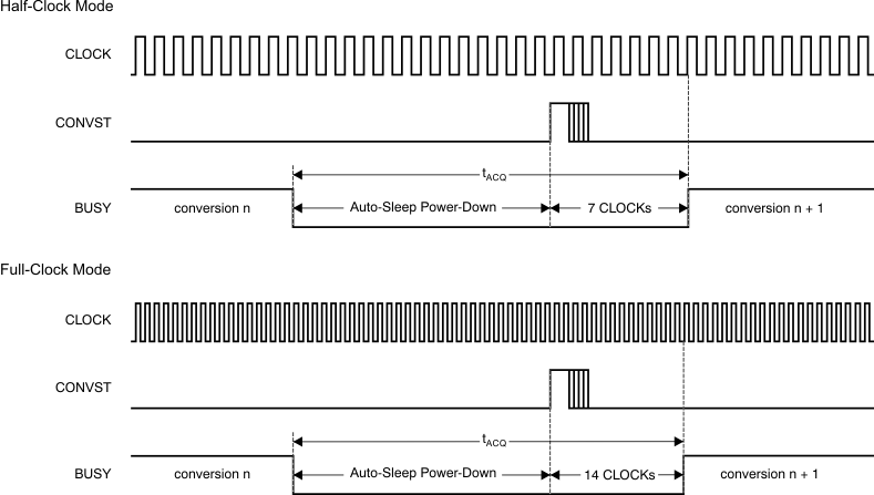 Figure 30. Actual Conversion Start In Auto-Sleep Mode
8.4.1.4 Reset
To issue a device reset, an RD pulse must be generated along with a control word containing A[3:0] = '0100'. With the completion of this write access, the entire device including the serial interface is forced into reset, interrupting any ongoing conversions, setting the input into acquisition mode, and returning the register contents to their default values. After approximately 20 ns, the serial interface becomes active again. The device also supports an automatic power-up reset (POR) that ensures proper (default) settings of the device.
8.5 Programming
8.5.1 Read Data Input (RD)
The RD input is used to control serial data outputs SDOx. The falling edge of the RD pulse triggers the output of the first bit of the output data. When CID = '0', the first bit of output data on SDOx is the analog input channel indicator; when CID = '1', the first bit of output data on SDOx is the MSB of the conversion result, or the 15th bit of the selected register, followed by output bits that are updated with the rising edge of the CLOCK in half-clock mode, or falling edge of the CLOCK in full-clock mode.
The RD input can be controlled separately or in combination with the CONVST input (see Figure 48 for a detailed timing diagram of this case). If RD is controlled separately, RD can be issued whenever a conversion process is finished (that is, after the falling edge of BUSY). However, in order to achieve the maximum data rate, the conversion results must be read during an ongoing conversion. In this case, the RD pulse must not be issued between the 16th and 19th clock cycle in half-clock mode, or between the 34th and 36th clock cycle in full-clock mode, after starting the conversion.
If a read access is repeated without issuing a new conversion, the result of the last conversion is presented on the outputs again. A repeated readout must only be performed when BUSY is low.
Note that in full-clock mode, only the first read access delivers the correct channel information (if CID = '0' in the CONFIG register), when the following readouts contain invalid channel details. The channel information is corrected with the next conversion.
Read access to verify the content of the internal registers is described in the Register Maps section.
8.5.2 Serial Data Outputs (SDOx)
The following sections explain the different modes of operation in detail.
The digital output code format of the ADS8363, ADS7263, and ADS7223 is binary twos complement, as shown in Table 7.
Consider both detailed timing diagrams (Figure 1 and Figure 2) illustrated in Figure 1 and Figure 2. For maximum data throughput, the description and diagrams given in this document assume that the CONVST and RD pins are tied together; see Figure 48 for timing details in this case. Note that these pins can also be controlled independently.
Table 7. Output Data Format
8.5.2.1 Mode I
With the M0 and M1 pins both set to '0', the device enters manual channel-control operation and outputs data on both SDOA and SDOB, accordingly. The SDI pin can be used to switch between the channels, as explicitly shown in the corresponding timing diagrams. A conversion is initiated by bringing CONVST high.
With the rising edge of CONVST, the device switches asynchronously to the external CLOCK from sample to hold mode, and the BUSY output pin goes high and remains high for the duration of the conversion cycle. On the falling edge of the second CLOCK cycle, the device latches in the channel for the next conversion cycle, depending on the status of CONFIG register bits C[1:0]. CS must be brought low to enable both serial outputs. Data are valid on the falling edge of every 20 clock cycles per conversion. The first two bits are set to '0'. The subsequent data contain the 16-, 14-, or 12-bit conversion result (the most significant bit is transferred first), with trailing zeroes, as shown in Figure 31.
This mode can be used for fully- or pseudo-differential inputs; in both cases, channel information bits are '00' if CID = '0'. Note that FIFO is not available in this mode.
8.5.2.2 Mode II (Half-Clock Mode Only)
With M0 = '0' and M1 = '1', the ADS8363, ADS7263, and ADS7223 also operate in manual channel-control mode and output data on the SDOA pin only when SDOB is set to high impedance. All other pins function in the same manner as they do in Mode I.
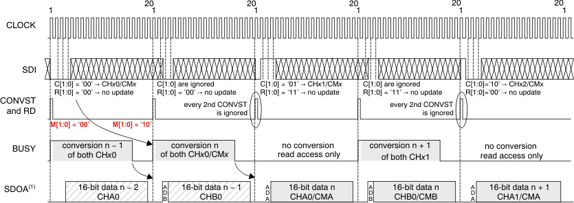
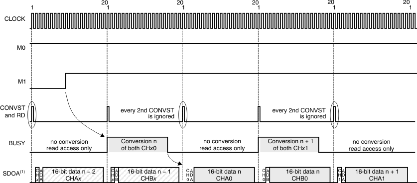
In half-clock mode, because 40 clock cycles are required to output the results from both ADCs (instead of 20 cycles if M1 = '0'), the device requires 2.0 μs to perform a complete read cycle. If the CONVST signal is issued every 1.0 μs (required for the RD signal) as in Mode I, every second pulse is ignored, as shown in Figure 32. CONVST and RD signals must not be longer than one clock cycle to ensure proper functionality and avoid corruption of output data.
Full-clock mode is not supported in this operational mode.
The output data consist of a '0', followed by an ADC indicator ('0' for CHAx or '1' for CHBx), and then 16, 14, or 12 bits of conversion result along with any trailing zeroes.
This mode can be used for fully- or pseudo-differential inputs. Channel information is valid in fully-differential mode only if CID = '0' (CID contains correct ADC information when the channel bit is invalid in pseudo-differential mode). Note that FIFO is not available in this mode.
Changes to register bits FE, SR, PDE, and CID are active with the start of the next conversion. with a delay of one read access.
The register settings must be updated using every other RD pulse, aligned either with the one starting the conversion or the one to read the conversion results of channel B, as shown in Figure 32.
8.5.2.3 Special Read Mode II (Half-Clock Mode Only)
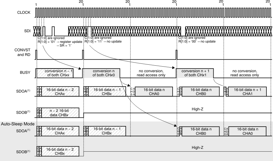
For Mode II, a special read mode is available in the ADS8363, ADS7263, and ADS7223 where both data results can be read out triggered by a single RD pulse (see Figure 33). To activate this mode, The SR bit in the CONFIG register must be set to '1' (see Table 8). The CONVST and RD pins can still be tied together but are issued every 40 CLOCK cycles instead of 20. Output data are presented on SDOA only when SDOB is held in 3-state.
The RD signal in this mode must not be longer than one clock cycle to avoid corruption of output data.
This special mode can be used for fully- or pseudo-differential inputs. Channel information is valid in fully-differential mode only if CID = '0' (CID contains correct ADC information when the channel bit is invalid in pseudo-differential mode). Note that FIFO is not available in this mode.
8.5.2.4 Mode III
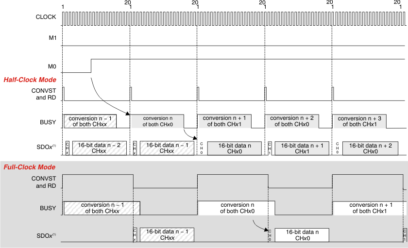
With M0 = '1' and M1 = '0', the device automatically cycles between the differential inputs (CONFIG register bits C[1:0] are ignored) when offering the conversion result of CHAx on SDOA and the conversion result of CHBx on SDOB, as shown in Figure 34.
Output data consist of a channel indicator ('0' for CHx0, or '1' for CHx1), followed by a '0', and then 16, 14, or 12 bits of conversion result along with any trailing zeroes.
This mode can be used for fully- or pseudo-differential inputs (in pseudo-differential mode the sequencer is used to control the input multiplexer). Channel information is available in fully-differential mode only if CID = '0' (CID is forced to '1' in pseudo-differential mode).
The internal FIFO is available in this mode; when used, a single read pulse allows for reading of all stored conversion data. The FIFO must be completely filled when used for the first time in order to ensure proper functionality.
8.5.2.5 Fully-Differential Mode IV (Half-Clock Mode Only)
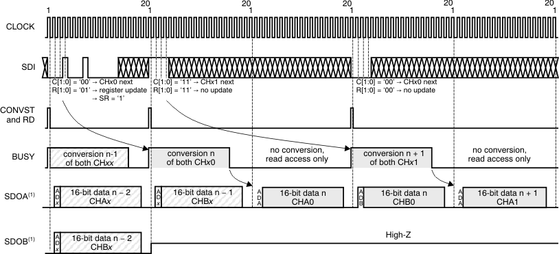
In the same way as Mode II, Mode IV uses the SDOA output line exclusively to transmit data when the differential channels are switched automatically. Following the first conversion after M1 goes high, the SDOB output 3-states, as shown in Figure 35.
Output data consist of a channel indicator ('0' for CHx0, or '1' for CHx1), followed by the ADC indicator ('0' for CHAx or '1' for CHBx), and then 16 or 14 bits of conversion result, ending with '00' for the ADS8363, '0000' for the ADS7263, or '000000' for the ADS7223.
CONVST and RD signals must not be longer than one clock cycle to ensure proper functionality and avoid corruption of output data.
Full-clock mode is not supported in this operational mode.
Channel information is available in fully-differential mode if CID = '0'. In pseudo-differential mode, the sequencer controls the channel selection in this mode and must be set appropriately using the SEQFIFO register. The internal FIFO is not available in this mode.
Changes to CONFIG register bits FE, SR, PDE, and CID are active with the start of the next conversion with a delay of one read access.
The register settings must be updated using every other RD pulse (aligned either with the one starting the conversion or the one to read the conversion results of channel B; compare with Figure 32).
8.5.2.6 Special Mode IV (Half-Clock Mode Only)
As with Special Mode II, these devices also offer a special read mode for Mode IV, where both data results of a conversion can be read by triggering a single RD pulse, as shown in Figure 36. Additionally, in this case, the SR bit in the CONFIG register must be set to '1' and the CONVST and RD pins can still be tied together, but are issued every 40 CLOCK cycles instead of 20. The RD signal in this mode must not be longer than one clock cycle to avoid corruption of output data.
Data are available on the SDOA pin, accordingly.
If auto-sleep power-down mode is enabled, the conversion results are presented during the next conversion, as shown in Figure 36.
This mode can be used for fully- or pseudo-differential inputs (note that in pseudo-differential mode, the sequencer is used to control the input multiplexer); channel information is available if CID = '0' in fully-differential mode only (CID forced to '1' in pseudo-differential mode).
The internal FIFO is available in this mode; when used, a single read pulse allows for reading of all stored conversion data. The FIFO must be completely filled when used for the first time in order to ensure proper functionality.
8.5.3 Programming the Reference DAC
The internal reference DACs can be set by issuing an RD pulse when providing an control word with R[1:0] = '01' and A[3:0] = 'X010' or 'X101', depending on which DAC is going to be updated. Thereafter, a second RD pulse must be generated with a control word that starts with the first five bits being ignored followed by the reference power control and the corresponding 10-bit DAC value, as shown in Figure 37.
To verify the DACs settings, an RD pulse must be generated when providing a control word containing R[1:0] = '01' and A[3:0] = '0011' or '0110' to initialize the read access of the appropriate DAC register. Triggering the RD line again causes the SDOA output to provide the 16-bit DAC register value followed by '0000', if channel information is disabled (CID = '1'). When channel information is enabled (CID = '0'), the first two bits of the data output contain the currently selected analog input channel indicator ('0' for CHx0 or '1' for CHx1), followed by the 16-bit DAC register contents and an additional '00'. Although the register contents are valid on SDOA, the conversion result of channel Ax is lost (if a conversion was performed in parallel), the conversion result of channel Bx is valid on SDOB (if enabled), and data on SDI are ignored, as shown in Figure 37).
The default value of the DAC registers after power-up is 7FFh, corresponding to a disabled reference voltage of 2.5 V on both REFIOx pins.
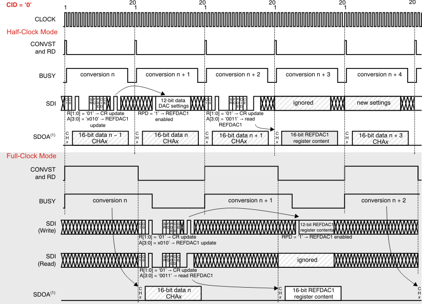 Figure 37. DAC Register Write and Read Access Timing
(Both SDOx Active and CID = '0')
8.6 Register Maps
The ADS8363, ADS7263, and ADS7223 operation is controlled through a set of registers described in the following sections. Table 8 shows the register map. The contents of these 16-bit registers can be set using the serial data input (SDI) pin, which is coupled to RD and clocked into the device on each falling edge of CLOCK. All data must be transferred MSB first. All register updates become active with the rising edge of CLOCK after completing the 16-clock-cycle write access operation.
Table 8. Register Map
| REGISTER | BIT 15 |
BIT 14 |
BIT 13 |
BIT 12 |
BIT 11 |
BIT 10 |
BIT 9 |
BIT 8 |
BIT 7 |
BIT 6 |
BIT 5 |
BIT 4 |
BIT 3 |
BIT 2 |
BIT 1 |
BIT 0 |
|---|---|---|---|---|---|---|---|---|---|---|---|---|---|---|---|---|
| CONFIG | C1 | C0 | R1 | R0 | PD1 | PD0 | FE | SR | FC | PDE | CID | CE | A3 | A2 | A1 | A0 |
| REFDAC1 | 0 | 0 | 0 | 0 | 0 | RPD | D9 | D8 | D7 | D6 | D5 | D4 | D3 | D2 | D1 | D0 |
| REFDAC2 | 0 | 0 | 0 | 0 | 0 | RPD | D9 | D8 | D7 | D6 | D5 | D4 | D3 | D2 | D1 | D0 |
| SEQFIFO | S1 | S0 | SL1 | SL0 | C11 | C10 | C21 | C20 | C31 | C30 | C41 | C40 | SP1 | SP0 | FD1 | FD0 |
| REFCM | CMB3 | CMB2 | CMB1 | CMB0 | CMA3 | CMA2 | CMA1 | CMA0 | RB3 | RB2 | RB1 | RB0 | RA3 | RA2 | RA1 | RA0 |
To update the CONFIG register, a single write access is required. To update the contents of all the other registers, a write access to the control register with the appropriate register address (bits A[3:0]), followed by a write access to the actual register is required, as shown in Figure 38. The CONFIG register contents can be updated when issuing a register read out access with a single register write access. For example, the mode of the device can be changed to full-clock mode when activating the REFDAC1 register read access; because full-clock mode is active upon the 16th clock cycle of the CONFIG register update, the REFDAC1 data are then presented according to the full-clock mode timing.
To verify the register contents, a read access can be issued using CONFIG register bits A[3:0]. Such access is described in the Programming the Reference DAC section, based on an example of verifying the reference DAC register settings. The register contents are always available on SDOA with the next read command. For example, if the FIFO is used, the register contents are presented after completion of the FIFO read access (see Table 9 for more details). In both cases, a complete read or write access requires a total of 40 clock cycles, during which a new access to the CONFIG register is not allowed.
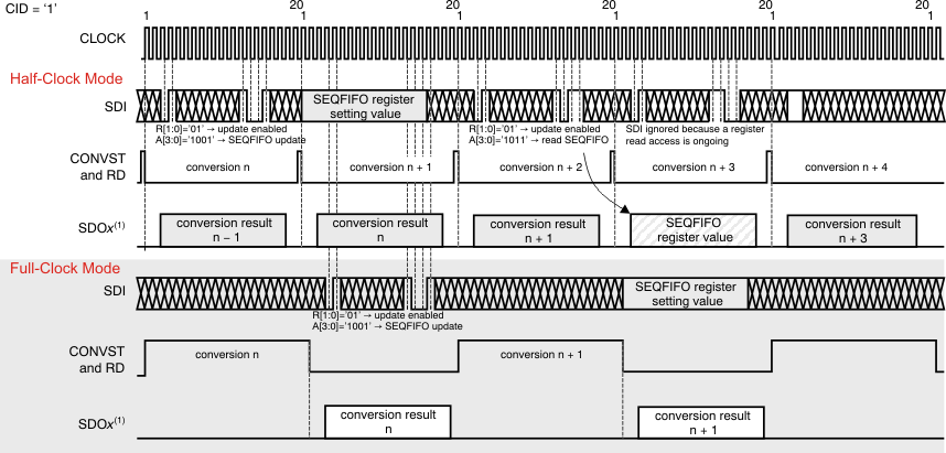
(Example: Half-Clock Mode, CID = '1')
8.6.1 Configuration (Config) Register
The configuration register selects the input channel, the activation of power-down modes, and the access to the sequencer and FIFO, reference selection, and reference DAC registers.
| 15 (MSB) | 14 | 13 | 12 | 11 | 10 | 9 | 8 | 7 | 6 | 5 | 4 | 3 | 2 | 1 | 0 (LSB) |
| C1 | C0 | R1 | R0 | PD1 | PD0 | FE | SR | FC | PDE | CID | CE | A3 | A2 | A1 | A0 |
| Bits[15:14] | C[1:0]—Input Channel Selection (ADS8361-compatible).
These bits control the multiplexer input selection depending on the status of the PDE bit. |
|
| If PDE = '0' (default), the multiplexer is in fully-differential mode and bits C[1:0] control the input multiplexer in the following manner: 0x = conversion of analog signals at inputs CHx0P/CHx0N (default). 1x = conversion of analog signals at inputs CHx1P/CHx1N. |
||
| If PDE = '1', the multiplexer is in pseudo-differential mode and bits C[1:0] control the input multiplexer in the following manner: 00 = conversion of analog signal at input CHx0 versus the selected CMx or REFIOx (default). 01 = conversion of analog signal at input CHx1 versus the selected CMx or REFIOx. 10 = conversion of analog signal at input CHx2 versus the selected CMx or REFIOx. 11 = conversion of analog signal at input CHx3 versus the selected CMx or REFIOx. |
||
| Bits[13:12] | R[1:0]—Configuration register update control.
These bits control the access to the CONFIG register. |
|
| 00 = If M0 = '0', update of input selection bits C[1:0] only (ADS8361-compatible behavior); if M0 = '1', no action (default). 01 = Update of the entire CONFIG register content enabled. 10 = Reserved for factory test; do not use. Changes may result in false behavior of the device. 11 = If M0 = '0', update of input selection bits C[1:0] only (ADS8361-compatible behavior); if M0 = '1', no action. |
||
| Bits[11:10] | PD[1:0]—Power-down control.
These bits control the different power-down modes of the device. |
|
| 00 = Normal operation (default). 01 = Device is in power-down mode (see the Power-Down Modes and Reset section for details). 10 = Device is in sleep power-down mode (see the Power-Down Modes and Reset section for details). 11 = Device is in Auto-sleep power-down mode (see the Power-Down Modes and Reset section for details). |
||
| Bit 9 | FE—FIFO enable control. | |
| 0 = The internal FIFO is disabled (default). 1 = The internal FIFO is enabled. The depth of the FIFO is controlled by SEQFIFO register bits FD[1:0]. |
||
| Bit 8 | SR—Special read mode control. | |
| 0 = Special read mode is disabled (default). 1 = Special read mode is enabled; see Figure 33 and Figure 36 for details. |
||
| Bit 7 | FC—Full clock mode operation control. | |
| 0 = Full-clock mode operation is disabled (default); see Figure 1 for details. 1 = Full-clock mode operation is enabled; see Figure 2 for details. |
||
| Bit 6 | PDE—Pseudo-differential mode operation enable. | |
| 0 = 2 x 2 fully-differential operation (default). 1 = 4 x 2 pseudo-differential operation. |
||
| Bit 5 | CID—Channel information disable. | |
| 0 = The channel information followed by conversion results or register contents are present on SDOx (default). 1 = Conversion data or register content is present on SDOx immediately after the falling edge of RD. |
||
| Bit 4 | CE—2-bit counter enable (see Figure 40). | |
| 0: The internal counter is disabled (default). 1: The counter value is available prior to the conversion result on SDOx (active only if CID = '0'). |
||
| Bits[3:0] | A[3:0]—Register access control.
These bits allow reading of the CONFIG register contents and control the access to the remaining registers of the device. |
|
| x000 = Update CONFIG register contents only (default) 0001 = Read CONFIG register content on SDOA with next access (see Figure 38). x010 = Write to REFDAC1 register with next access (see Figure 38). 0011 = Read REFDAC1 register content on SDOA with next access (see Figure 38). 0100 = Generate software reset of the device. x101 = Write to REFDAC2 register with next access (see Figure 38). 0110 = Read REFDAC2 register content on SDOA with next access (see Figure 38). x111 = Update CONFIG register contents only. 1001 = Write to SEQFIFO register with next access (see Figure 38). 1011 = Read SEQFIFO register content on SDOA with next access (see Figure 38). 1100 = Write to REFCM register with next access (see Figure 38). 1110 = Read REFCM register content on SDOA with next access (see Figure 38). |
||
8.6.2 REFDAC1 and REFDAC2 Registers
Two reference DAC registers allow for enabling and setting up the appropriate value for each of the output string DACs that are connected to the REFIO1 and REFIO2 pins.
| 15 (MSB) | 14 | 13 | 12 | 11 | 10 | 9 | 8 | 7 | 6 | 5 | 4 | 3 | 2 | 1 | 0 (LSB) |
| 0 | 0 | 0 | 0 | 0 | RPD | D9 | D8 | D7 | D6 | D5 | D4 | D3 | D2 | D1 | D0 |
| 15 (MSB) | 14 | 13 | 12 | 11 | 10 | 9 | 8 | 7 | 6 | 5 | 4 | 3 | 2 | 1 | 0 (LSB) |
| 0 | 0 | 0 | 0 | 0 | RPD | D9 | D8 | D7 | D6 | D5 | D4 | D3 | D2 | D1 | D0 |
| Bits[15:11] | Not used; always set to '0'. | |
| Bit 10 | RPD—DAC2 power down. | |
| 0 = Internal reference path 2 is enabled and the reference voltage is available at the REFIO2 pin. 1 = The internal reference path is disabled (default). |
||
| Bits[9:0] | D[9:0]—DAC2 setting bits. | |
| These bits correspond to the settings of the internal reference DACs (compare REFIO section). The D9 bit is the MSB value of the DAC. Default value is 3FFh (2.5V nom) |
||
8.6.3 Sequencer/FIFO (SEQFIFO) Register
The ADS8363, ADS7363, and ADS7223 feature a programmable sequencer that controls the switching of the ADC input multiplexer in pseudo-differential, automatic channel-selection mode only. When used, a single read pulse allows reading of all stored conversion data. A single CONVST is required to control the conversion of the entire sequence. If the sequencer is used, CONVST and RD must be controlled independently (see Figure 44 and Figure 45).
Additionally, a programmable FIFO is available on each channel that allows for storing up to four conversion results. Both features are controlled using this register. If FIFO is used, CONVST and RD must be controlled independently. Note that after activation of this feature, the FIFO must be full before being read for the first time.
If the FIFO is full and a new conversion starts, the contents are shifted by one and the oldest result is lost. Only when the sequencer is used are the entire FIFO contents lost (that is, all bits are automatically set to '0'). The FIFO can be used independently from the sequencer. When both are used, the complete sequence must be finished before reading the data out of the FIFO; otherwise, the data may be corrupted.
Table 9 contains details of the data readout requirements depending on the FIFO settings in automatic channel selection mode.
Table 9. Conversion Result Read Out In FIFO Mode
| AUTOMATIC CHANNEL SELECTION | ||
|---|---|---|
| INPUT SIGNAL TYPE | FE = '0' | FE = '1' |
| Fully-differential input mode | Read cycle length = 1 word One RD pulse required after each conversion |
Read cycle length = 2 · FIFO length One RD pulse required for the entire FIFO content |
| Pseudo-differential input mode | Read cycle length = 1 word One RD pulse required after each conversion or after completing the sequence if S1 = '1' and S0 = '1' |
Read cycle length = 2 · sequencer length · FIFO length One RD pulse required for the entire FIFO content |
| 15 (MSB) | 14 | 13 | 12 | 11 | 10 | 9 | 8 | 7 | 6 | 5 | 4 | 3 | 2 | 1 | 0 (LSB) |
| S1 | S0 | SL1 | SL0 | C11 | C10 | C21 | C20 | C31 | C30 | C41 | C40 | SP1 | SP0 | FD1 | FD0 |
| Bits[15:14] | S[1:0]—Sequencer mode selection (see Figure 44) in pseudo-differential mode only.
These bits allow for the control of the number of CONVSTs required, and the behavior of the BUSY pin in Sequencer mode. |
|
| 0x = An individual CONVST is required with BUSY indicating each conversion (default). 10 = A single CONVST is required for the entire sequence with BUSY indicating each conversion (half-clock mode only). 11 = A single CONVST is required for the entire sequence with BUSY remaining high throughout the sequence (half-clock mode only) |
||
| Bits[13:12] | SL[1:0] Sequencer length control.
These bits control the length of a sequence. Bits [11:6] are only active if SL > '00'. |
|
| 00 = Do not use; use Mode I or II instead, where M0 = '0' (default). 01 = Sequencer length = 2; C1x (bits[11:10]) and C2x (bits[9:8]) define the actual channel selection. 10 = Sequencer length = 3; C1x (bits[11:10]), C2x (bits[9:8]) and C3x (bits[7:6]) define the actual channel selection. 11 = Sequencer length = 4; C1x (bits[11:10]), C2x (bits[9:8]), C3x (bits[7:6]), and C4x (bits[5:4]) define the actual channel selection. |
||
| Bits[11:10] | C1[1:0]—First channel in sequence selection bits. | |
| Bits[9:8] | C2[1:0]—Second channel in sequence selection bits. | |
| Bits[7:6] | C3[1:0]—Third channel in sequence selection bits. | |
| Bits[5:4] | C4[1:0]—Fourth channel in sequence selection bits. | |
| Bits [11:4] control the pseudo-differential input multiplexer channel selection in sequencer mode. | ||
| 00 = CHA0 and CHB0 are selected for the next conversion (default). 01 = CHA1 and CHB1 are selected for the next conversion. 10 = CHA2 and CHB2 are selected for the next conversion. 11 = CHA3 and CHB3 are selected for the next conversion. |
||
| Bits[3:2] | SP[1:0]—Sequence position bits (read only).
These bits indicate the setting of the pseudo-differential input multiplexer in sequencer mode. |
|
| 00 = Inputs selected using bits C1[1:0] are converted with next rising edge of CONVST (default). 01 = Inputs selected using bits C2[1:0] are converted with next rising edge of CONVST. 10 = Inputs selected using bits C3[1:0] are converted with next rising edge of CONVST. 11 = Inputs selected using bits C4[1:0] are converted with next rising edge of CONVST. |
||
| Bits [1:0] | FD[1:0]—FIFO depth control (see Figure 45).
These bits control the depth of the internal FIFO if CONFIG register bit FE = '1'. |
|
| 00 = One conversion result per channel is stored in the FIFO for burst read access (default). 01 = Two conversion results per channel are stored in the FIFO for burst read access. 10 = Three conversion results per channel are stored in the FIFO for burst read access. 11 = Four conversion results per channel are stored in the FIFO for burst read access . |
||
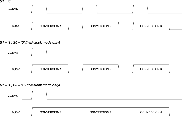 Figure 44. Sequencer Modes
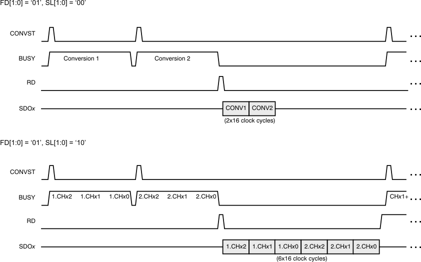 Figure 45. FIFO and Sequencer Operation Example
8.6.4 Reference and Common-Mode Selection (REFCM) Register
To allow flexible adjustment of the common-mode voltage in pseudo-differential mode when simplifying the circuit layout, the ADS8363, ADS7263, and ADS7223 provide this register to assign one of the CMx inputs as a reference for each of the input signals. According to the register settings, the CMx signals are internally connected to the appropriate negative input of each ADC.
Additionally, this register also allows for the flexible assignment of one of the internal reference DAC outputs as a reference for each channel in both fully- and pseudo-differential modes.
| 15 (MSB) | 14 | 13 | 12 | 11 | 10 | 9 | 8 | 7 | 6 | 5 | 4 | 3 | 2 | 1 | 0 (LSB) |
| CMB3 | CMB2 | CMB1 | CMB0 | CMA3 | CMA2 | CMA1 | CMA0 | RB3 | RB2 | RB1 | RB0 | RA3 | RA2 | RA1 | RA0 |
| Bits[15:8] | CMxx—Common-mode source selection bits (per input channel).
These bits allow selection of the CMx input pins or the internal reference source as common-mode for pseudo-differential inputs B[3:0] and A[3:0]. The selected signal is connected to the negative input of the corresponding ADC. |
|
| 0 = external common-mode source through CMx (default). 1 = internal common-mode source = REFIOx, depending on settings of bits Rx[3 :0]. |
||
| Bit 7 | RB3—Internal reference DAC output selection for CHB3 in pseudo-differential mode, or channel CHB1P, CHB1N in fully-differential mode. | |
| 0 = internal reference source REFIO1 selected (default). 1 = internal reference source REFIO2 selected. |
||
| Bit 6 | RB2—Internal reference DAC output selection for CHB2 in pseudo-differential mode only. | |
| 0 = internal reference source REFIO1 selected (default). 1 = internal reference source REFIO2 selected. |
||
| Bit 5 | RB1—Internal reference DAC output selection for CHB1 in pseudo-differential mode only. | |
| 0 = internal reference source REFIO1 selected (default). 1 = internal reference source REFIO2 selected. |
||
| Bit 4 | RB0—Internal reference DAC output selection for CHB0 in pseudo-differential mode, or channel CHB0P, CHB0N in fully-differential mode. | |
| 0 = internal reference source REFIO1 selected (default). 1 = internal reference source REFIO2 selected. |
||
| Bit 3 | RA3—Internal reference DAC output selection for CHA3 in pseudo-differential mode, or channel CHA1P, CHA1N in fully-differential mode. | |
| 0 = internal reference source REFIO1 selected (default). 1 = internal reference source REFIO2 selected. |
||
| Bit 2 | RA2—Internal reference DAC output selection for CHA2 in pseudo-differential mode only. | |
| 0 = internal reference source REFIO1 selected (default). 1 = internal reference source REFIO2 selected. |
||
| Bit 1 | RA1—Internal reference DAC output selection for CHA1 in pseudo-differential mode only. | |
| 0 = internal reference source REFIO1 selected (default). 1 = internal reference source REFIO2 selected. |
||
| Bit 0 | RA0—Internal reference DAC output selection for CHA0 in pseudo-differential mode, or channel CHA0P, CHA0N in fully-differential mode. | |
| 0 = internal reference source REFIO1 selected (default). 1 = internal reference source REFIO2 selected. |
||
