SLUSB80E September 2012 – January 2018
PRODUCTION DATA.
- 1 Features
- 2 Applications
- 3 Description
- 4 Revision History
- 5 Description (Continued)
- 6 Device Comparisons
- 7 Pin Configuration and Functions
- 8 Specifications
-
9 Detailed Description
- 9.1 Overview
- 9.2 Functional Block Diagrams
- 9.3 Operational Flow Chart
- 9.4 Feature Description
- 9.5 Device Functional Modes
- 9.6 Programming
- 9.7 Register Description
- 10Application and Implementation
- 11Power Supply Recommendations
- 12Layout
- 13Device and Documentation Support
- 14Mechanical, Packaging, and Orderable Information
Package Options
Mechanical Data (Package|Pins)
- YFF|20
Thermal pad, mechanical data (Package|Pins)
Orderable Information
1 Features
- Power Up System without Battery
- Charge Faster than Linear Chargers
- High-Accuracy Voltage and Current Regulation
- Input Current Regulation Accuracy: ±5% (100 mA and 500 mA)
- Charge Voltage Regulation Accuracy: ±0.5% (25°C), ±1% (0°C to 125°C)
- Charge Current Regulation Accuracy: ±5%
- Input Voltage Based Dynamic Power Management (VIN DPM)
- Bad Adaptor Detection and Rejection
- Safety Limit Register for Maximum Charge Voltage and Current Limiting
- High-Efficiency Mini-USB/AC Battery Charger for Single-Cell Li-Ion and Li-Polymer Battery Packs
- 20-V Absolute Maximum Input Voltage Rating
- 6.5-V Maximum Operating Input Voltage
- Built-In Input Current Sensing and Limiting
- Integrated Power FETs for Up To 1.55-A Charge Rate
- Programmable Charge Parameters through I2C™ Compatible Interface (up to 3.4 Mbps):
- Input Current Limit
- VIN DPM Threshold
- Fast-Charge/Termination Current
- Charge Regulation Voltage (3.5 V to 4.44 V)
- Low Charge Current Mode Enable/Disable
- Termination Enable/Disable
- Support up to 1.55A Charge Current using 55 mΩ Sensing Resistor
- Synchronous Fixed-Frequency PWM Controller Operating at 3 MHz With 0% to 99.5% Duty Cycle
- Automatic High Impedance Mode for Low Power Consumption
- Robust Protection
- Reverse Leakage Protection Prevents Battery Drainage
- Thermal Regulation and Protection
- Input/Output Overvoltage Protection
- Status Output for Charging and Faults
- USB Friendly Boot-Up Sequence
- Automatic Charging
- Boost Mode Operation for USB OTG
- Input Voltage Range (from Battery): 3.2 V to 4.5 V
- 2.1 mm x 2 mm 20-Pin WCSP Package
2 Applications
- Mobile and Smart Phones
- MP3 Players
- Handheld Devices
3 Description
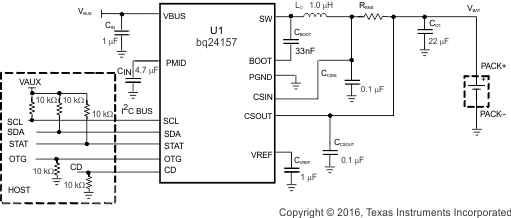
The bq24157 is a compact, flexible, high-efficiency, USB-friendly switch-mode charge management device for single-cell Li-ion and Li-polymer batteries used in a wide range of portable applications. The charge parameters can be programmed through an I2C interface. The IC integrates a synchronous PWM controller, power MOSFETs, input current sensing, high-accuracy current and voltage regulation, and charge termination, into a small WCSP package.
Device Information(1)
| PART NUMBER | PACKAGE | BODY SIZE (NOM) |
|---|---|---|
| bq24157 | WCSP (20-Pin) | 2.1 mm x 2.0 mm |
- For all available packages, see the orderable addendum at the end of the datasheet.
4 Revision History
Changes from D Revision (July 2016) to E Revision
- Changed Output voltage (with respect to PGND) - SW MIN value From: –0.7 To: –2 in the Absolute Maximum RatingsGo
- Deleted graphs "Cycle by Cycle Current Limiting in Charge Mode" and "PWM Charging Waveform" from the Typical CharacteristicsGo
- Deleted list item "Default charge current will be 550 mA, if 68-mΩ sensing resistor is used, since default LOW_CHG = 0." following Table 8Go
Changes from B Revision (October 2013) to C Revision
- Added ESD Ratings table, Timing Requirements table, Feature Description section, Device Functional Modes, Application and Implementation section, Power Supply Recommendations section, Layout section, Device and Documentation Support section, and Mechanical, Packaging, and Orderable Information sections.Go
- Changed Features From: Integrated Power FETs for Up To 1.25-A To: Integrated Power FETs for Up To 1.55-AGo
- Changed the ICHARGE(MAX) row of the Device Comparisons table.Go
- Changed capacitor from 10-nF to 33-nF for BOOT pin in the Pin Functions table Go
- Changed Note 1 in the Electrical Characteristics table From: "While in 15-min mode" To: "While in DEFAULT mode"Go
- Deleted "t15M, 15 minute safety timer" in the Electrical Characteristics tableGo
- Changed Figure 3 "15 Minute Mode" To: "DEFAULT Mode" and "32 S Mode" To" HOST Mode"Go
- Changed Figure 8 text note From: "32S mode" To: "HOST MODE" Go
- Changed Figure 14Go
- Added Battery Detection at Power Up in DEFAULT Mode Go
- Changed section 15-Minute Safety Timer To: DEFAULT Mode Go
- Added Figure 26 and Figure 27Go
- Changed section title From: Design considerations and potential issues: To: Design Requirements and Potential Issues:Go
Changes from A Revision (March 2013) to B Revision
- Changed Table 8 Memory location: 05, Bit B5 Function description from "....(default 0)" to ".....(default 1)Go
Changes from * Revision (September 2012) to A Revision
