SLUSBU3B February 2014 – December 2016
PRODUCTION DATA.
- 1 Features
- 2 Applications
- 3 Description
- 4 Revision History
- 5 Description (Continued)
- 6 Pin Configuration and Functions
- 7 Specifications
-
8 Detailed Description
- 8.1 Overview
- 8.2 Functional Block Diagram
- 8.3
Feature Description
- 8.3.1 Device Power Up
- 8.3.2 Power Path Management
- 8.3.3 Battery Charging Management
- 8.3.4 Status Outputs (PG, STAT, and INT)
- 8.3.5 Protections
- 8.4 Device Functional Modes
- 8.5 Programming
- 8.6
Register Map
- 8.6.1
I2C Registers
- 8.6.1.1 Input Source Control Register REG00 [reset = 00110xxx, or 3x]
- 8.6.1.2 Power-On Configuration Register REG01 [reset = 00011011, or 0x1B]
- 8.6.1.3 Charge Current Control Register REG02 [reset = 01100000, or 60]
- 8.6.1.4 Pre-Charge/Termination Current Control Register REG03 [reset = 00010001, or 0x11]
- 8.6.1.5 Charge Voltage Control Register REG04 [reset = 10110010, or 0xB2]
- 8.6.1.6 Charge Termination/Timer Control Register REG05 [reset = 10011100, or 0x9C]
- 8.6.1.7 Boost Voltage/Thermal Regulation Control Register REG06 [reset = 01110011, or 0x73]
- 8.6.1.8 Misc Operation Control Register REG07 [reset = 01001011, or 4B]
- 8.6.1.9 System Status Register REG08
- 8.6.1.10 New Fault Register REG09
- 8.6.1.11 Vender / Part / Revision Status Register REG0A
- 8.6.1
I2C Registers
- 9 Application and Implementation
- 10Power Supply Recommendations
- 11Layout
- 12Device and Documentation Support
- 13Mechanical, Packaging, and Orderable Information
Package Options
Mechanical Data (Package|Pins)
- RGE|24
Thermal pad, mechanical data (Package|Pins)
- RGE|24
Orderable Information
1 Features
- 90% High Efficiency Switch Mode 3-A Charger
- 3.9-V to 6.2-V Single Input USB-Compliant Charger with 6.4-V Over-Voltage Protection
- Input voltage and current limit supports USB 2.0 and USB 3.0
- Input Current Limit: 100 mA, 150 mA, 500 mA, 900 mA, 1 A, 1.5 A, 2 A, and 3 A
- USB OTG with Adjustable output 4.55 V to 5.5 V at 1 A or 1.5 A
- Fast OTG Startup (22 ms Typ)
- 90% 5-V Boost Mode Efficiency
- Accurate ±15% Hiccup Mode Overcurrent Protection
- Narrow VDC (NVDC) Power Path Management
- Instant System On with No Battery or Deeply Discharged Battery
- Ideal Diode Operation in Battery Supplement Mode
- 1.5-MHz Switching Frequency for Low Profile 1.2-mm Inductor
- I2C port for optimal system performance and status reporting
- Autonomous Battery Charging with or without Host Management
- Battery Charge Enable
- Battery Charge Preconditioning
- Charge Termination and Recharge
- High Accuracy
- ±0.5% Charge Voltage Regulation
- ±7% Charge Current Regulation
- ±7.5% Input Current Regulation
- ±3% Output Voltage Regulation in USB OTG Boost Mode
- High Integration
- Power Path Management
- Synchronous Switching MOSFETs
- Integrated Current Sensing
- Bootstrap Diode
- Internal Loop Compensation
- Safety
- Battery Temperature Sensing for Charging and Discharging in OTG Mode
- Battery Charging Safety Timer
- Thermal Regulation and Thermal Shutdown
- Input and System Over-Voltage Protection
- MOSFET Over-Current Protection
- Charge Status Outputs for LED or Host Processor
- Maximum power tracking capability by input voltage regulation
- 20-µA Low Battery Leakage Current and Support Shipping Mode
- 4-mm x 4-mm VQFN-24 Package
2 Applications
- Tablet PC, Smart Phone, Internet Devices
- Portable Audio Speaker
3 Description
The bq24296M is a highly-integrated switch-mode battery charge management and system power path management device for 1 cell Li-Ion and Li-polymer battery in a wide range of smart phone and tablet applications. Its low impedance power path optimizes switch-mode operation efficiency, reduces battery charging time and extends battery life during discharging phase. The I2C serial interface with charging and system settings makes the device a truly flexible solution.
Device Information(1)
| PART NUMBER | PACKAGE | BODY SIZE (NOM) |
|---|---|---|
| bq24296M | VQFN (24) | 4.00 mm x 4.00 mm |
- For all available packages, see the orderable addendum at the end of the data sheet.
4 Revision History
Changes from A Revision (January 2015) to B Revision
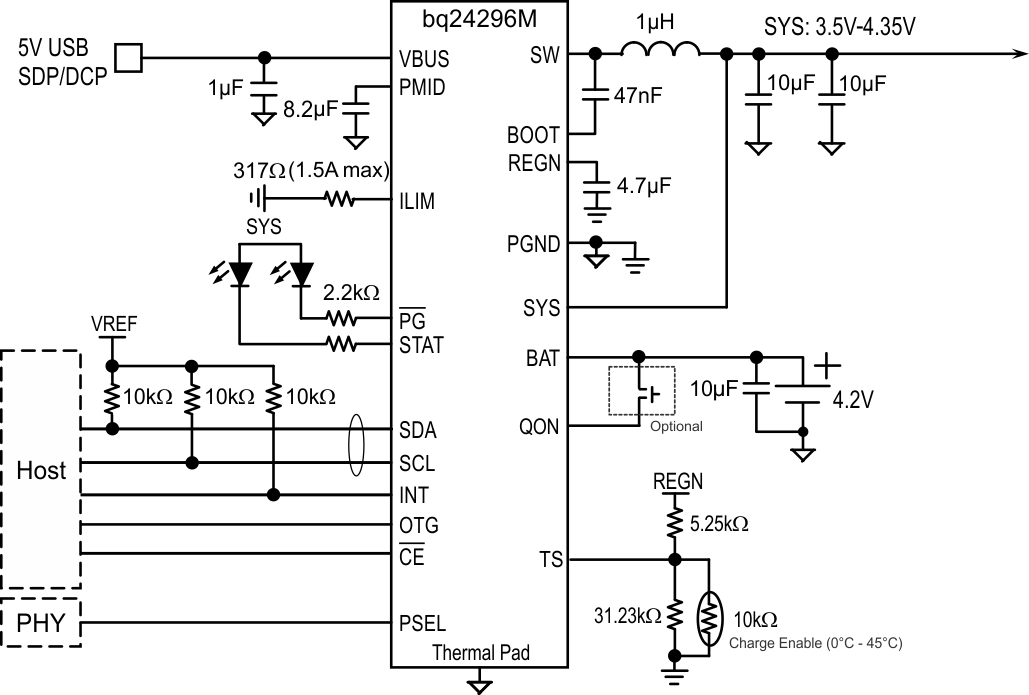
- Changed VREF to VREGN in Figure 17 Go
- Changed 20°C to –20°C and VREF to VREGN in Figure 18 Go
- Changed Equation 1 Go
- Changed Bit 3 RESET from 1 to 0 in Table 10 Go
- Changed Bit 2 RESET from 1 to 0 in Table 10 Go
- Changed 0 to 1 for REG05 Bit 2 Reset in Table 11 Go
- Changed 1 to 0 for REG05 Bit 1 Reset in Table 11 Go
- Added note to Figure 39 Go
- Changed last paragraph in Output Capacitor sectionGo
Changes from * Revision (February 2014) to A Revision
- Added ESD Ratings table, Feature Description section, Device Functional Modes, Application and Implementation section, Power Supply Recommendations section, Layout section, Device and Documentation Support section, and Mechanical, Packaging, and Orderable Information section.Go
- Changed 5.52kΩ to 5.25kΩ in PSEL from PHY, Charging from SDP/DCP, and Optional BATFET Enable Interface Go
- Changed Power Pad to Thermal Pad throughout data sheetGo
- Added (10k NTC thermistor only) to QON descriptionGo
- Changed falling to rising in VHTF in Electrical CharacteristicsGo
- Added VIH_OTG to Electrical CharacteristicsGo
- Deleted wavefroms from Typical Characteristics and added to Application Performance PlotsGo
- Added The status register REG08[0] goes high when the system is in minimum system voltage regulation to 2nd paragraph in Narrow VDC ArchitectureGo
- Changed last paragraph of Narrow VDC ArchitectureGo
- Deleted and LSFET from Voltage and Current Monitoring in Buck Mode descriptionGo
- Deleted HSFET and from Voltage and Current Monitoring in Boost Mode descriptionGo
- Deleted HSFET (Q2) from 1st paragraph in Over-Current Protection Go
- Changed REG09[5] to REG09[3] in Battery Over-Voltage Protection (BATOVP)Go
- Changed REG05 reset from 10011010, or 0x9A to 10011100, or 0x9CGo
- Changed REG09 Bit 3 description 1 – System OVP to Battery OVP Go
- Changed paragraph in Application Information Go
- Changed 5.52kΩ to 5.25kΩ in Figure 39 Go
