-
BQ24392 Dual SPST USB 2.0 High Speed Switch with USB Battery Charging Specification Revision 1.2 Detection
- 1 Features
- 2 Applications
- 3 Description
- 4 Revision History
- 5 Pin Configuration and Functions
- 6 Specifications
- 7 Detailed Description
- 8 Application and Implementation
- 9 Power Supply Recommendations
- 10Layout
- 11Device and Documentation Support
- 12Mechanical, Packaging, and Orderable Information
- IMPORTANT NOTICE
Package Options
Mechanical Data (Package|Pins)
- RSE|10
Thermal pad, mechanical data (Package|Pins)
Orderable Information
BQ24392 Dual SPST USB 2.0 High Speed Switch with USB Battery Charging Specification Revision 1.2 Detection
1 Features
- USB 2.0 High Speed Switch
- Detects USB Battery Charging Specification Version 1.2 (BCv1.2) Compliant Chargers
- Compatible Accessories
- Dedicated Charging Port
- Standard Downstream Port
- Charging Downstream Port
- Non-Standard Chargers
- Apple™ Charger
- TomTom™ Charger
- USB Chargers Not Compliant With Battery Charging Specification Version 1.2 (BCv1.2)
- –2 V to 28 V VBUS Voltage Range
- ESD Performance Tested per JESD 22
- 4000-V Human-Body Model
- 1500-V Charged-Device Model (C101)
- ESD Performance DP_CON/DM_CON to GND
- ±8-kV Contact Discharge (IEC 61000-4-2)
2 Applications
- Mobile Phones
- Smart Phones
- Cameras
- GPS Systems
3 Description
The BQ24392 is a dual single-pole single-throw (SPST) USB 2.0 high-speed isolation switch with charger detection capabilities for use with micro and mini-USB ports. This USB switch allows mobile phones, tablets, and other battery operated electronics to be charged from different adapters with minimal system software. The device’s charger detection circuitry can support USB Battery Charging Specification version 1.2 (BCv1.2) compliant, Apple™, TomTom™, and other non-standard chargers.
The BQ24392 device is powered through VBUS when a charger is attached to the micro or mini-USB port and has a 28-V tolerance to avoid the need for external protection.
Device Information(1)
| PART NUMBER | PACKAGE | BODY SIZE (NOM) |
|---|---|---|
| BQ24392 | UQFN (10) | 2.05 mm × 1.55 mm |
- For all available packages, see the orderable addendum at the end of the datasheet.
SPACER
SPACER
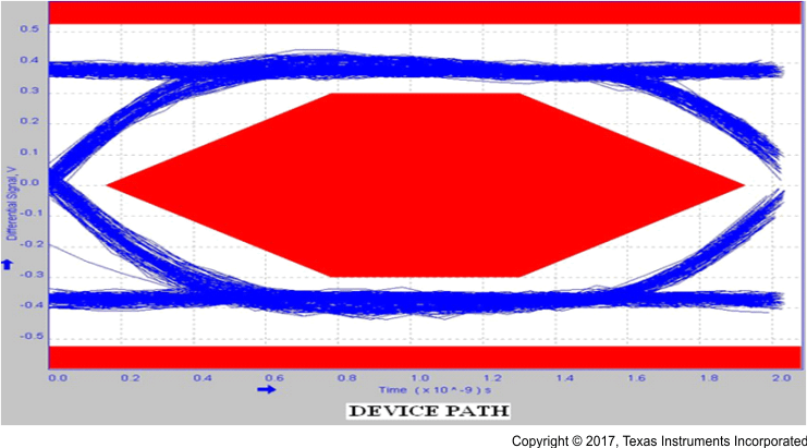
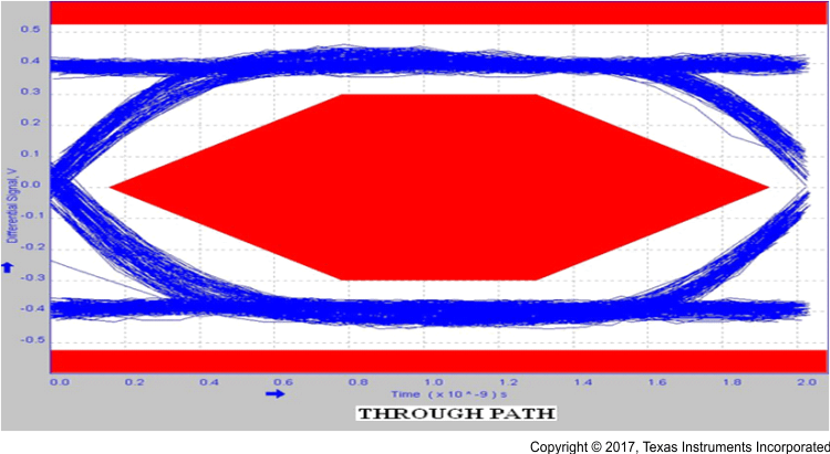
480-Mbps USB 2.0 Eye Diagram With USB Switch

4 Revision History
Changes from F Revision (July 2017) to G Revision
- Changed RON From: 8 Ω TYP To: 3.5 Ω TYP, 6.9 Ω MAX in the Electrical Characteristic table Go
Changes from E Revision (February 2017) to F Revision
- Changed CHG_DET diode direction from right facing to left facing in Application Schematic. Go
Changes from D Revision (January 2016) to E Revision
- Changed From: BQ24932 To: BQ24392 in the DescriptionGo
- Changed From: BQ24932 To: BQ24392 in the OverviewGo
- Changed title From: Using the BQ24932 GPIOs To: Using the BQ24392 GPIOsGo
Changes from C Revision (January 2015) to D Revision
- Changed diode direction from left facing to right facing in Application Schematic. Go
Changes from B Revision (October 2014) to C Revision
- Updated Features. Go
Changes from A Revision (June 2012) to B Revision
- Added ESD Rating table, Feature Description section, Device Functional Modes, Application and Implementation section, Power Supply Recommendations section, Layout section, Device and Documentation Support section, and Mechanical, Packaging, and Orderable Information section. Go
5 Pin Configuration and Functions

Pin Functions
| PIN | I/O | DESCRIPTION | |
|---|---|---|---|
| NO. | NAME | ||
| 1 | SW_OPEN | O | USB switch status indicator Open-drain output. 10kΩ external pull-up resistor required SW_OPEN = LOW indicates when switch is connected SW_OPEN = HIGH-Z indicates when then switch is not connected |
| 2 | DM_HOST | I/O | D– signal to transceiver |
| 3 | DP_HOST | I/O | D+ signal to transceiver |
| 4 | CHG_AL_N | O | Charging status indicator Open-drain output. 10kΩ external pull-up resistor required CHG_AL_N = LOW indicates when charging is allowed CHG_AL_N = HIGH-Z indicates when charging is not allowed |
| 5 | GOOD_BAT | I | Battery status indication from system GOOD_BAT = LOW indicates a dead battery GOOD_BAT = HIGH indicates a good battery |
| 6 | GND | - | Ground |
| 7 | DP_CON | I/O | D+ signal from USB connector |
| 8 | DM_CON | I/O | D– signal from USB connector |
| 9 | VBUS | I | Supply pin from USB connector |
| 10 | CHG_DET | O | Charger detection indicator Push-Pull output to system CHG_DET = LOW indicates when a charger is not detected CHG_DET = HIGH indicates when a charger detected |
6 Specifications
6.1 Absolute Maximum Ratings
over –40℃ to 85℃ temperature range (unless otherwise noted)| MIN | MAX | UNIT | ||
|---|---|---|---|---|
| Input Voltage | VBUS | –2 | 28 | V |
| CHG_AL_N | –2 | 28 | V | |
| DM_HOST | –0.3 | 7 | V | |
| DP_HOST | –0.3 | 7 | ||
| GOOD_BAT | –0.3 | 7 | ||
| DP_CON | –0.3 | 7 | ||
| DM_CON | –0.3 | 7 | ||
| CHG_DET | –0.3 | 7 | ||
| Tstg | Storage temperature range | 65 | 150 | °C |
6.2 ESD Ratings
| VALUE | UNIT | |||
|---|---|---|---|---|
| V(ESD) | Electrostatic discharge | Human-body model (HBM), per ANSI/ESDA/JEDEC JS-001(1) | ±4000 | V |
| Charged-device model (CDM), per JEDEC specification JESD22-C101(2) | ±1500 | |||
| IEC Contact discharge pins DP_CON and DM_CON to GND | ±8000 | |||
6.3 Recommended Operating Conditions
| MIN | MAX | UNIT | ||
|---|---|---|---|---|
| VBUS | 4.75 | 5.25 | V | |
| GOOD_BAT | 0 | VBUS | ||
| DM_HOST | 0 | 3.6 | ||
| DP_HOST | 0 | 3.6 | ||
| DM_CON | 0 | 3.6 | ||
| DP_CON | 0 | 3.6 | ||
6.4 Thermal Information
| THERMAL METRIC(1) | bq24392 | UNIT | |
|---|---|---|---|
| RSE | |||
| 10 PINS | |||
| RθJA | Junction-to-ambient thermal resistance | 167.7 | °C/W |
| RθJC(top) | Junction-to-case (top) thermal resistance | 78.8 | °C/W |
| RθJB | Junction-to-board thermal resistance | 95.8 | °C/W |
| ψJT | Junction-to-top characterization parameter | 4.7 | °C/W |
| ψJB | Junction-to-board characterization parameter | 95.9 | °C/W |
6.5 Electrical Characteristics
VBUS = 4.5 V to 5.5 V, TA = –40°C to 85°C (unless otherwise noted)(1)6.6 Typical Characteristics

