-
BQ24725A SMBus 1- to 4-Cell Li+ Buck Battery Charge Controller with N-Channel Power MOSFET Selector
- 1 Features
- 2 Applications
- 3 Description
- 4 Revision History
- 5 Pin Configuration and Functions
- 6 Specifications
- 7 Parameter Measurement Information
-
8 Detailed Description
- 8.1 Overview
- 8.2 Functional Block Diagram
- 8.3 Feature Description
- 8.4
Device Functional Modes
- 8.4.1 Adapter Detect and ACOK Output
- 8.4.2 Adapter Over Voltage (ACOVP)
- 8.4.3 System Power Selection
- 8.4.4 Battery LEARN Cycle
- 8.4.5 Enable and Disable Charging
- 8.4.6 Automatic Internal Soft-Start Charger Current
- 8.4.7 High Accuracy Current Sense Amplifier
- 8.4.8 Charge Timeout
- 8.4.9 Converter Operation
- 8.4.10 Continuous Conduction Mode (CCM)
- 8.4.11 Discontinuous Conduction Mode (DCM)
- 8.4.12 Input Over Current Protection (ACOC)
- 8.4.13 Charge Over Current Protection (CHGOCP)
- 8.4.14 Battery Over Voltage Protection (BATOVP)
- 8.4.15 Battery Shorted to Ground (BATLOWV)
- 8.4.16 Thermal Shutdown Protection (TSHUT)
- 8.4.17 EMI Switching Frequency Adjust
- 8.4.18 Inductor Short, MOSFET Short Protection
- 8.5 Register Maps
-
9 Application and Implementation
- 9.1 Application Information
- 9.2
Typical Applications
- 9.2.1
Typical System with Two NMOS Selector
- 9.2.1.1 Design Requirements
- 9.2.1.2
Detailed Design Procedure
- 9.2.1.2.1 Negative Output Voltage Protection
- 9.2.1.2.2 Reverse Input Voltage Protection
- 9.2.1.2.3 Reduce Battery Quiescent Current
- 9.2.1.2.4 Inductor Selection
- 9.2.1.2.5 Input Capacitor
- 9.2.1.2.6 Output Capacitor
- 9.2.1.2.7 Power MOSFETs Selection
- 9.2.1.2.8 Input Filter Design
- 9.2.1.2.9 BQ24725A Design Guideline
- 9.2.1.3 Application Curves
- 9.2.2 Simplified System without Power Path
- 9.2.1
Typical System with Two NMOS Selector
- 9.3 System Examples
- 10Power Supply Recommendations
- 11Layout
- 12Device and Documentation Support
- 13Mechanical, Packaging, and Orderable Information
- IMPORTANT NOTICE
Package Options
Mechanical Data (Package|Pins)
- RGR|20
Thermal pad, mechanical data (Package|Pins)
- RGR|20
Orderable Information
BQ24725A SMBus 1- to 4-Cell Li+ Buck Battery Charge Controller with N-Channel Power MOSFET Selector
1 Features
- SMBus Host-controlled NMOS-NMOS synchronous buck converter with programmable 615kHz, 750kHz, and 885kHz switching frequencies
- Automatic N-channel MOSFET selection of system power source from adapter or battery driven by internal charge pumps
- Enhanced safety features for over voltage protection, over current protection, battery, inductor and MOSFET short circuit protection
- Programmable input current, charge voltage, charge current limits
- ±0.5% Charge voltage accuracy up to 19.2V
- ±3% Charge current accuracy up to 8.128A
- ±3% Input current accuracy up to 8.064A
- ±2% 20x Adapter current or charge current amplifier output accuracy
- Programmable battery depletion threshold, and battery LEARN function
- Programmable adapter detection and indicator
- Integrated soft start
- Integrated loop compensation
- Real time system control on ILIM pin to limit charge current
- AC Adapter operating range 4.5V-24V
- 5µA Off-state battery discharge current
- 0.65mA (0.8mA max) Adapter standby quiescent current
- 20-pin 3.5 x 3.5 mm2 VQFN Package
2 Applications
- Portable notebook computers, UMPC, Ultra-thin notebook, and Netbook
- Handheld terminal
- Industrial and medical equipment
- Portable equipment
3 Description
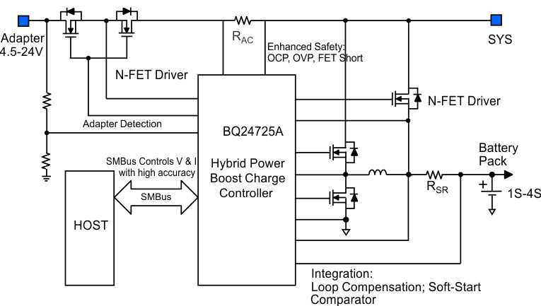
The BQ24725A is a high-efficiency, synchronous battery charger, offering low component count for space-constraint, multi-chemistry battery charging applications.
The BQ24725A utilizes two charge pumps to separately drive n-channel MOSFETs (ACFET, RBFET and BATFET) for automatic system power source selection.
SMBus controlled input current, charge current, and charge voltage DACs allow for very high regulation accuracies that can be easily programmed by the system power management micro-controller.
The BQ24725A uses internal input current register or external ILIM pin to throttle down PWM modulation to reduce the charge current.
The BQ24725A charges one, two, three or four series Li+ cells.
- For all available packages, see the orderable addendum at the end of the datasheet.

4 Revision History
Changes from B Revision (November 2018) to C Revision
- Changed Title Go
- Added Description for Figure 18Go
- Added Simplified System without Power Path sectionGo
Changes from A Revision (August 2014) to B Revision
- Changed Handling Ratings To: ESD RatingsGo
- Moved Tstg From: Handling Ratings table To: Absolute Maximum RatingsGo
- Added the Application NOTE Go
- Changed the Notes to Figure 27 for additional resistor requirement to the application circuit when using low VGS input FETs Go
Changes from * Revision (September 2011) to A Revision