Completely Offloads Wi-Fi and Internet Protocols from the Application Microcontroller
Start your design with the industry’s first Wi-Fi CERTIFIED single-chip microcontroller unit (MCU) with built-in Wi-Fi connectivity. Created for the Internet of Things (IoT), the SimpleLink CC3200 device is a wireless MCU that integrates a high-performance ARM Cortex-M4 MCU, allowing customers to develop an entire application with a single IC. With on-chip Wi-Fi, Internet, and robust security protocols, no prior Wi-Fi experience is required for faster development. The CC3200 device is a complete platform solution including software, sample applications, tools, user and programming guides, reference designs, and the TI E2E™ support community. The device is available in a QFN package that is easy to layout.
The applications MCU subsystem contains an industry-standard ARM Cortex-M4 core running at 80 MHz. The device includes a wide variety of peripherals, including a fast parallel camera interface, I2S, SD/MMC, UART, SPI, I2C, and four-channel ADC. The CC3200 family includes flexible embedded RAM for code and data and ROM with external serial flash bootloader and peripheral drivers.
The Wi-Fi network processor subsystem features a Wi-Fi Internet-on-a-Chip and contains an additional dedicated ARM MCU that completely offloads the applications MCU. This subsystem includes an 802.11 b/g/n radio, baseband, and MAC with a powerful crypto engine for fast, secure Internet connections with 256-bit encryption. The CC3200 device supports Station, Access Point, and Wi-Fi Direct modes. The device also supports WPA2 personal and enterprise security and WPS 2.0. The Wi-Fi Internet-on-a-chip includes embedded TCP/IP and TLS/SSL stacks, HTTP server, and multiple Internet protocols.
The power-management subsystem includes integrated DC-DC converters supporting a wide range of supply voltages. This subsystem enables low-power consumption modes, such as the hibernate with RTC mode requiring less than 4 μA of current.
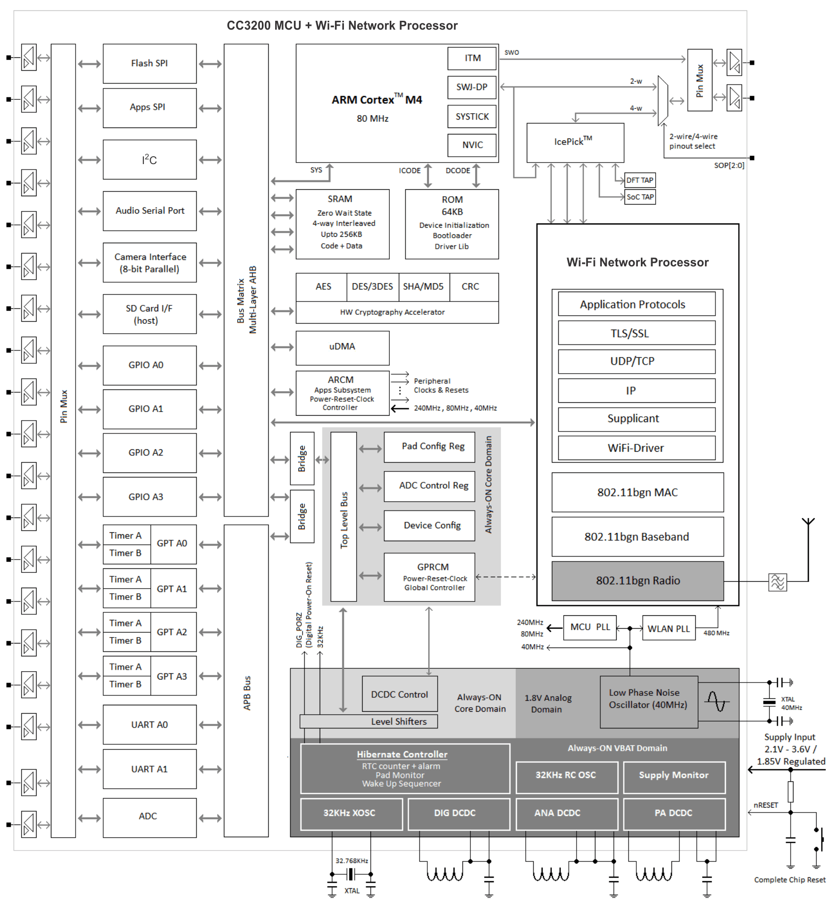
Figure 1-1 shows the CC3200 hardware overview.
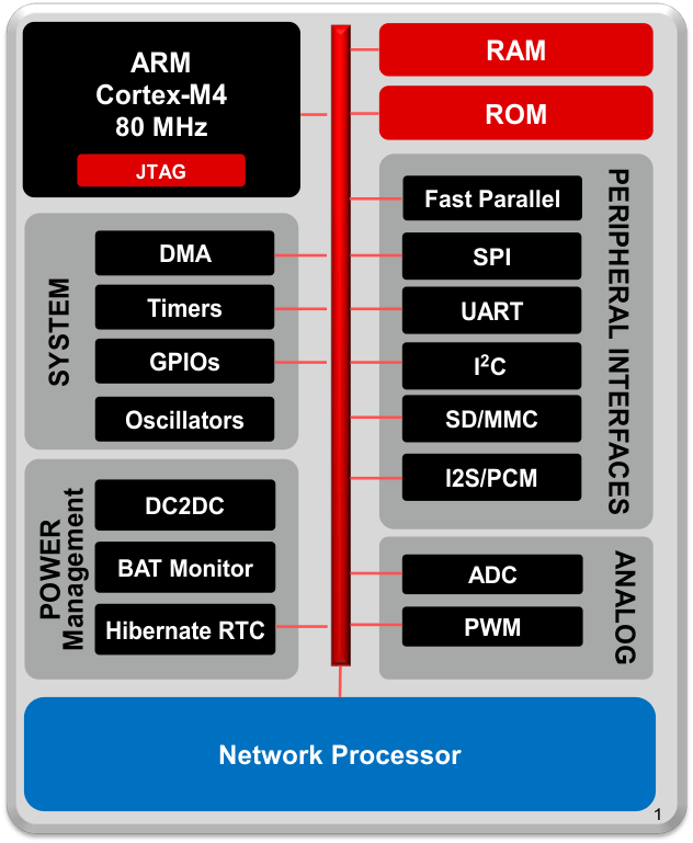
Figure 1-2 shows an overview of the CC3200 embedded software.
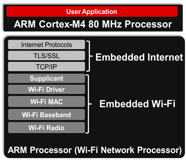
Figure 1-3 shows a block diagram of the CC3200 device.
Changes from E Revision (August 2014) to F Revision
Figure 3-1 shows pin assignments for the 64-pin QFN package.
The device makes extensive use of pin multiplexing to accommodate the large number of peripheral functions in the smallest possible package. To achieve this configuration, pin multiplexing is controlled using a combination of hardware configuration (at device reset) and register control.
NOTE
TI highly recommends using the CC3200 pin multiplexing utility to obtain the desired pinout.
The board and software designers are responsible for the proper pin multiplexing configuration. Hardware does not ensure that the proper pin multiplexing options are selected for the peripherals or interface mode used.
Table 3-1 describes the general pin attributes and presents an overview of pin multiplexing. All pin multiplexing options are configurable using the pin mux registers.
The following special considerations apply:
NOTE
If an external device drives a positive voltage to the signal pads and the CC3200 device is not powered, DC current is drawn from the other device. If the drive strength of the external device is adequate, an unintentional wakeup and boot of the CC3200 device can occur. To prevent current draw, TI recommends any one of the following:
General Pin Attributes | Function | Pad States | |||||||||||
---|---|---|---|---|---|---|---|---|---|---|---|---|---|
Pkg Pin | Pin Alias | Use | Select as Wakeup Source | Config Addl Analog Mux | Muxed with JTAG | Dig. Pin Mux Config Reg | Dig. Pin Mux Config Mode Value | Signal Name | Signal Description | Signal Direction | LPDS(1) | Hib(2) | nRESET = 0 |
1 | GPIO10 | I/O | No | No | No | GPIO_PAD_CONFIG_10 (0x4402 E0C8) |
0 | GPIO10 | General-Purpose I/O | I/O | Hi-Z | Hi-Z | Hi-Z |
1 | I2C_SCL | I2C Clock | O (Open Drain) |
Hi-Z | |||||||||
3 | GT_PWM06 | Pulse-Width Modulated O/P | O | Hi-Z | |||||||||
7 | UART1_TX | UART TX Data | O | 1 | |||||||||
6 | SDCARD_CLK | SD Card Clock | O | 0 | |||||||||
12 | GT_CCP01 | Timer Capture Port | I | Hi-Z | |||||||||
2 | GPIO11 | I/O | Yes | No | No | GPIO_PAD_CONFIG_11 (0x4402 E0CC) |
0 | GPIO11 | General-Purpose I/O | I/O | Hi-Z | Hi-Z | Hi-Z |
1 | I2C_SDA | I2C Data | I/O (Open Drain) |
Hi-Z | |||||||||
3 | GT_PWM07 | Pulse-Width Modulated O/P | O | Hi-Z | |||||||||
4 | pXCLK (XVCLK) | Free Clock To Parallel Camera | O | 0 | |||||||||
6 | SDCARD_CMD | SD Card Command Line | I/O | Hi-Z | |||||||||
7 | UART1_RX | UART RX Data | I | Hi-Z | |||||||||
12 | GT_CCP02 | Timer Capture Port | I | Hi-Z | |||||||||
13 | McAFSX | I2S Audio Port Frame Sync | O | Hi-Z | |||||||||
3 | GPIO12 | I/O | No | No | No | GPIO_PAD_CONFIG_12 (0x4402 E0D0) |
0 | GPIO12 | General Purpose I/O | I/O | Hi-Z | Hi-Z | Hi-Z |
3 | McACLK | I2S Audio Port Clock O | O | Hi-Z | |||||||||
4 | pVS (VSYNC) | Parallel Camera Vertical Sync | I | Hi-Z | |||||||||
5 | I2C_SCL | I2C Clock | I/O (Open Drain) |
Hi-Z | |||||||||
7 | UART0_TX | UART0 TX Data | O | 1 | |||||||||
12 | GT_CCP03 | Timer Capture Port | I | Hi-Z | |||||||||
4 | GPIO13 | I/O | Yes | No | No | GPIO_PAD_CONFIG_13 (0x4402 E0D4) |
0 | GPIO13 | General-Purpose I/O | I/O | Hi-Z | Hi-Z | Hi-Z |
5 | I2C_SDA | I2C Data | I/O (Open Drain) |
||||||||||
4 | pHS (HSYNC) | Parallel Camera Horizontal Sync | I | ||||||||||
7 | UART0_RX | UART0 RX Data | I | ||||||||||
12 | GT_CCP04 | Timer Capture Port | I | ||||||||||
5 | GPIO14 | I/O | No | No | GPIO_PAD_CONFIG_14 (0x4402 E0D8) |
0 | GPIO14 | General-Purpose I/O | I/O | Hi-Z | Hi-Z | Hi-Z | |
5 | I2C_SCL | I2C Clock | I/O (Open Drain) |
||||||||||
7 | GSPI_CLK | General SPI Clock | I/O | ||||||||||
4 | pDATA8 (CAM_D4) | Parallel Camera Data Bit 4 | I | ||||||||||
12 | GT_CCP05 | Timer Capture Port | I | ||||||||||
6 | GPIO15 | I/O | No | No | GPIO_PAD_CONFIG_15 (0x4402 E0DC) |
0 | GPIO15 | General-Purpose I/O | I/O | Hi-Z | Hi-Z | Hi-Z | |
5 | I2C_SDA | I2C Data | I/O (Open Drain) |
||||||||||
7 | GSPI_MISO | General SPI MISO | I/O | ||||||||||
4 | pDATA9 (CAM_D5) | Parallel Camera Data Bit 5 | I | ||||||||||
13 | GT_CCP06 | Timer Capture Port | I | ||||||||||
8 | SDCARD_ DATA0 |
SD Card Data | I/O | ||||||||||
7 | GPIO16 | I/O | No | No | GPIO_PAD_CONFIG_16 (0x4402 E0E0) |
0 | GPIO16 | General-Purpose I/O | I/O | Hi-Z | Hi-Z | Hi-Z | |
Hi-Z | |||||||||||||
7 | GSPI_MOSI | General SPI MOSI | I/O | Hi-Z | |||||||||
4 | pDATA10 (CAM_D6) | Parallel Camera Data Bit 6 | I | Hi-Z | |||||||||
5 | UART1_TX | UART1 TX Data | O | 1 | |||||||||
13 | GT_CCP07 | Timer Capture Port | I | Hi-Z | |||||||||
8 | SDCARD_CLK | SD Card Clock | O | O | |||||||||
8 | GPIO17 | I/O | Wake-Up Source | No | No | GPIO_PAD_CONFIG_17 (0x4402 E0E4) |
0 | GPIO17 | General-Purpose I/O | I/O | Hi-Z | Hi-Z | Hi-Z |
5 | UART1_RX | UART1 RX Data | I | ||||||||||
7 | GSPI_CS | General SPI Chip Select | I/O | ||||||||||
4 | pDATA11 (CAM_D7) | Parallel Camera Data Bit 7 | I | ||||||||||
8 | SDCARD_ CMD |
SD Card Command Line | I/O | ||||||||||
9 | VDD_DIG1 | Int pwr | N/A | N/A | N/A | N/A | N/A | VDD_DIG1 | Internal Digital Core Voltage | ||||
10 | VIN_IO1 | Sup. input | N/A | N/A | N/A | N/A | N/A | VIN_IO1 | Chip Supply Voltage (VBAT) | ||||
11 | FLASH_SPI_ CLK |
O | N/A | N/A | N/A | N/A | N/A | FLASH_SPI_ CLK |
Clock To SPI Serial Flash (Fixed Default) | O | Hi-Z(3) | Hi-Z | Hi-Z |
12 | FLASH_SPI_DOUT | O | N/A | N/A | N/A | N/A | N/A | FLASH_SPI_ DOUT |
Data To SPI Serial Flash (Fixed Default) | O | Hi-Z(3) | Hi-Z | Hi-Z |
13 | FLASH_SPI_ DIN |
I | N/A | N/A | N/A | N/A | N/A | FLASH_SPI_ DIN |
Data From SPI Serial Flash (Fixed Default) | I | |||
14 | FLASH_SPI_ CS |
O | N/A | N/A | N/A | N/A | N/A | FLASH_SPI_ CS |
Chip Select To SPI Serial Flash (Fixed Default) | O | 1 | Hi-Z | Hi-Z |
15 | GPIO22 | I/O | No | No | No | GPIO_PAD_CONFIG_22 (0x4402 E0F8) |
0 | GPIO22 | General-Purpose I/O | I/O | Hi-Z | Hi-Z | Hi-Z |
7 | McAFSX | I2S Audio Port Frame Sync | O | Hi-Z | |||||||||
5 | GT_CCP04 | Timer Capture Port | I | ||||||||||
16 | TDI | I/O | No | No | MUXed with JTAG TDI | GPIO_PAD_CONFIG_23 (0x4402 E0FC) |
1 | TDI | JTAG TDI. Reset Default Pinout. | I | Hi-Z | Hi-Z | Hi-Z |
0 | GPIO23 | General-Purpose I/O | I/O | ||||||||||
2 | UART1_TX | UART1 TX Data | O | 1 | |||||||||
9 | I2C_SCL | I2C Clock | I/O (Open Drain) |
Hi-Z | |||||||||
17 | TDO | I/O | Wake-Up Source | No | MUXed with JTAG TDO | GPIO_PAD_CONFIG_ 24 (0x4402 E100) |
1 | TDO | JTAG TDO. Reset Default Pinout. | O | Hi-Z | Hi-Z | Hi-Z |
0 | GPIO24 | General-Purpose I/O | I/O | ||||||||||
5 | PWM0 | Pulse Width Modulated O/P | O | ||||||||||
2 | UART1_RX | UART1 RX Data | I | ||||||||||
9 | I2C_SDA | I2C Data | I/O (Open Drain) |
||||||||||
4 | GT_CCP06 | Timer Capture Port | I | ||||||||||
6 | McAFSX | I2S Audio Port Frame Sync | O | ||||||||||
18 | GPIO28 | I/O | No | GPIO_PAD_CONFIG_ 28 (0x4402 E110) |
0 | GPIO28 | General-Purpose I/O | I/O | Hi-Z | Hi-Z | Hi-Z | ||
19 | TCK | I/O | No | No | MUXed with JTAG/SWD-TCK | 1 | TCK | JTAG/SWD TCK Reset Default Pinout | I | Hi-Z | Hi-Z | Hi-Z | |
8 | GT_PWM03 | Pulse Width Modulated O/P | O | ||||||||||
20 | TMS | I/O | No | No | MUXed with JTAG/SWD-TMSC | GPIO_PAD_CONFIG_ 29 (0x4402 E114) |
1 | TMS | JATG/SWD TMS Reset Default Pinout | I/O | Hi-Z | Hi-Z | Hi-Z |
0 | GPIO29 | General-Purpose I/O | |||||||||||
21(4)(5) | SOP2 | O Only | No | No | No | GPIO_PAD_CONFIG_ 25 (0x4402 E104) |
0 | GPIO25 | General-Purpose I/O | O | Hi-Z | Driven Low | Hi-Z |
9 | GT_PWM02 | Pulse Width Modulated O/P | O | Hi-Z | |||||||||
2 | McAFSX | I2S Audio Port Frame Sync | O | Hi-Z | |||||||||
See (6) | TCXO_EN | Enable to Optional External 40-MHz TCXO | O | O | |||||||||
See (7) | SOP2 | Sense-On-Power 2 | I | ||||||||||
22 | WLAN_XTAL_N | WLAN Ana. | N/A | N/A | N/A | N/A | See (6) | WLAN_XTAL_N | 40-MHz XTAL Pulldown if ext TCXO is used. |
||||
23 | WLAN_XTAL_P | WLAN Ana. | N/A | N/A | N/A | N/A | WLAN_XTAL_P | 40-MHz XTAL or TCXO clock input | |||||
24 | VDD_PLL | Int. Pwr | N/A | N/A | N/A | N/A | VDD_PLL | Internal analog voltage | |||||
25 | LDO_IN2 | Int. Pwr | N/A | N/A | N/A | N/A | LDO_IN2 | Analog RF supply from ANA DC-DC output | |||||
26 | NC | WLAN Ana. | N/A | N/A | N/A | N/A | NC | Reserved | |||||
27 | NC | WLAN Ana. | N/A | N/A | N/A | N/A | NC | Reserved | |||||
28 | NC | WLAN Ana. | N/A | N/A | N/A | N/A | NC | Reserved | |||||
29(8) | ANTSEL1 | O Only | No | User config not required (9) |
No | GPIO_PAD_CONFIG_26 (0x4402 E108) |
0 | ANTSEL1(3) | Antenna Selection Control | O | Hi-Z | Hi-Z | Hi-Z |
30(8) | ANTSEL2 | O Only | No | User config not required (9) |
No | GPIO_PAD_CONFIG_27 (0x4402 E10C) |
0 | ANTSEL2(3) | Antenna Selection Control | O | Hi-Z | Hi-Z | Hi-Z |
31 | RF_BG | WLAN Ana. | N/A | N/A | N/A | N/A | RF_BG | RF BG band | |||||
32 | nRESET | Glob. Rst | N/A | N/A | N/A | N/A | nRESET | Master chip reset. Active low. | |||||
33 | VDD_PA_IN | Int. Pwr | N/A | N/A | N/A | N/A | VDD_PA_IN | PA supply voltage from PA DC-DC output. | |||||
34(5) | SOP1 | Config Sense | N/A | N/A | N/A | N/A | SOP1 | Sense On Power 1 | |||||
35(5) | SOP0 | Config Sense | N/A | N/A | N/A | N/A | SOP0 | Sense On Power 0 | |||||
36 | LDO_IN1 | Internal Power | N/A | N/A | N/A | N/A | LDO_IN1 | Analog RF supply from ana DC-DC output | |||||
37 | VIN_DCDC_ANA | Supply Input | N/A | N/A | N/A | N/A | VIN_DCDC_ ANA |
Analog DC-DC input (connected to chip input supply [VBAT]) | |||||
38 | DCDC_ANA_SW | Internal Power | N/A | N/A | N/A | N/A | DCDC_ANA_ SW |
Analog DC-DC switching node. | |||||
39 | VIN_DCDC_PA | Supply Input | N/A | N/A | N/A | N/A | VIN_DCDC_PA | PA DC-DC input (connected to chip input supply [VBAT]) | |||||
40 | DCDC_PA_SW_P | Internal Power | N/A | N/A | N/A | N/A | DCDC_PA_ SW_ P |
PA DCDC switching node | |||||
41 | DCDC_PA_SW_N | Internal Power | N/A | N/A | N/A | N/A | DCDC_PA_ SW_ N |
PA DCDC switching node | |||||
42 | DCDC_PA_OUT | Internal Power | N/A | N/A | N/A | N/A | DCDC_PA_ OUT |
PA buck converter output | |||||
43 | DCDC_DIG_SW | Internal Power | N/A | N/A | N/A | N/A | DCDC_DIG_ SW |
DIG DC-DC switching node | |||||
44 | VIN_DCDC_DIG | Supply Input | N/A | N/A | N/A | N/A | VIN_DCDC_ DIG |
DIG DC-DC input (connected to chip input supply [VBAT]) | |||||
45(10) | DCDC_ANA2_SW_P | I/O | No | User config not required (9)(11) |
No | GPIO_PAD_CONFIG_31 (0x4402 E11C) |
0 | GPIO31 | General-Purpose I/O | I/O | Hi-Z | Hi-Z | Hi-Z |
9 | UART0_RX | UART0 RX Data | I | ||||||||||
12 | McAFSX | I2S Audio Port Frame Sync | O | ||||||||||
2 | UART1_RX | UART1 RX Data | I | ||||||||||
6 | McAXR0 | I2S Audio Port Data 0 (RX/TX) | I/O | ||||||||||
7 | GSPI_CLK | General SPI Clock | I/O | ||||||||||
See (6) | DCDC_ANA2_ SW_P |
ANA2 DCDC Converter +ve Switching Node. | |||||||||||
46 | DCDC_ANA2_SW_N | Internal Power | N/A | N/A | N/A | N/A | N/A | DCDC_ANA2_ SW_N |
ANA2 DCDC Converter -ve Switching Node. | ||||
47 | VDD_ANA2 | Internal Power | N/A | N/A | N/A | N/A | N/A | VDD_ANA2 | ANA2 DCDC O | ||||
48 | VDD_ANA1 | Internal Power | N/A | N/A | N/A | N/A | N/A | VDD_ANA1 | Analog supply fed by ANA2 DCDC output | ||||
49 | VDD_RAM | Internal Power | N/A | N/A | N/A | N/A | N/A | VDD_RAM | SRAM LDO output | ||||
50 | GPIO0 | I/O | No | User config not required (9) |
No | GPIO_PAD_CONFIG_0 (0x4402 E0A0) |
0 | GPIO0 | General-Purpose I/O | I/O | Hi-Z | Hi-Z | Hi-Z |
12 | UART0_CTS | UART0 Clear To Send Input (Active Low) | I | Hi-Z | Hi-Z | Hi-Z | |||||||
6 | McAXR1 | I2S Audio Port Data 1 (RX/TX) | I/O | Hi-Z | |||||||||
7 | GT_CCP00 | Timer Capture Port | I | Hi-Z | |||||||||
9 | GSPI_CS | General SPI Chip Select | I/O | Hi-Z | |||||||||
10 | UART1_RTS | UART1 Request To Send O (Active Low) | O | 1 | |||||||||
3 | UART0_RTS | UART0 Request To Send O (Active Low) | O | 1 | |||||||||
4 | McAXR0 | I2S Audio Port Data 0 (RX/TX) | I/O | Hi-Z | |||||||||
51 | RTC_XTAL_P | RTC Clock | N/A | N/A | N/A | N/A | RTC_XTAL_P | Connect 32.768-kHz XTAL or Froce external CMOS level clock | |||||
52(10) | RTC_XTAL_N | O Only | User config not required (9)(12) |
No | GPIO_PAD_CONFIG_32 (0x4402 E120) |
RTC_XTAL_N | Connect 32.768-kHz XTAL or connect a 100 kΩ to Vsupply. | Hi-Z | Hi-Z | ||||
0 | GPIO32 | General-Purpose I/O | I/O | Hi-Z | |||||||||
2 | McACLK | I2S Audio Port Clock O | O | Hi-Z | |||||||||
4 | McAXR0 | I2S Audio Port Data (Only O Mode Supported On Pin 52) | O | Hi-Z | |||||||||
6 | UART0_RTS | UART0 Request To Send O (Active Low) | O | 1 | |||||||||
8 | GSPI_MOSI | General SPI MOSI | I/O | Hi-Z | |||||||||
53 | GPIO30 | I/O | No | User config not required (9) |
No | GPIO_PAD_CONFIG_30 (0x4402 E118) |
0 | GPIO30 | General-Purpose I/O | I/O | Hi-Z | Hi-Z | Hi-Z |
9 | UART0_TX | UART0 TX Data | O | 1 | |||||||||
2 | McACLK | I2S Audio Port Clock O | O | Hi-Z | |||||||||
3 | McAFSX | I2S Audio Port Frame Sync | O | Hi-Z | |||||||||
4 | GT_CCP05 | Timer Capture Port | I | Hi-Z | |||||||||
7 | GSPI_MISO | General SPI MISO | I/O | Hi-Z | |||||||||
54 | VIN_IO2 | Supply Input | N/A | N/A | N/A | N/A | VIN_IO2 | Chip Supply Voltage (VBAT) | |||||
55 | GPIO1 | I/O | No | No | No | GPIO_PAD_CONFIG_1 (0x4402 E0A4) |
0 | GPIO1 | General-Purpose I/O | I/O | Hi-Z | Hi-Z | Hi-Z |
3 | UART0_TX | UART0 TX Data | O | 1 | |||||||||
4 | pCLK (PIXCLK) | Pixel Clock From Parallel Camera Sensor | I | Hi-Z | |||||||||
6 | UART1_TX | UART1 TX Data | O | 1 | |||||||||
7 | GT_CCP01 | Timer Capture Port | I | Hi-Z | |||||||||
56 | VDD_DIG2 | Internal Power | N/A | N/A | N/A | N/A | VDD_DIG2 | Internal Digital Core Voltage | |||||
57(13) | GPIO2 | Analog Input (up to 1.8 V)/ Digital I/O | Wake-Up Source | See (10)(14) | No | GPIO_PAD_CONFIG_2 (0x4402 E0A8) |
See (6) | ADC_CH0 | ADC Channel 0 Input (1.5V max) | I | Hi-Z | Hi-Z | |
0 | GPIO2 | General-Purpose I/O | I/O | Hi-Z | |||||||||
3 | UART0_RX | UART0 RX Data | I | Hi-Z | |||||||||
6 | UART1_RX | UART1 RXt Data | I | Hi-Z | |||||||||
7 | GT_CCP02 | Timer Capture Port | I | Hi-Z | |||||||||
58(13) | GPIO3 | Analog Input (up to 1.8 V)/ Digital I/O | No | See (10)(14) | No | GPIO_PAD_CONFIG_3 (0x4402 E0AC) |
See (6) | ADC_CH1 | ADC Channel 1 Input (1.5V max) | I | Hi-Z | Hi-Z | |
0 | GPIO3 | General-Purpose I/O | I/O | Hi-Z | |||||||||
6 | UART1_TX | UART1 TX Data | O | 1 | |||||||||
4 | pDATA7 (CAM_D3) | Parallel Camera Data Bit 3 | I | Hi-Z | |||||||||
59(13) | GPIO4 | Analog Input (up to 1.8 V)/ Digital I/O | Wake-up Source | See (10)(14) | No | GPIO_PAD_CONFIG_4 (0x4402 E0B0) |
See (6) | ADC_CH2 | ADC Channel 2 Input (1.5V max) | I | Hi-Z | Hi-Z | |
0 | GPIO4 | General-Purpose I/O | I/O | Hi-Z | |||||||||
6 | UART1_RX | UART1 RX Data | I | Hi-Z | |||||||||
4 | pDATA6 (CAM_D2) | Parallel Camera Data Bit 2 | I | Hi-Z | |||||||||
60(13) | GPIO5 | Analog Input (up to 1.8 V)/ Digital I/O | No | See (10)(14) | No | GPIO_PAD_CONFIG_5 (0x4402 E0B4) |
See (6) | ADC_CH3 | ADC Channel 3 Input (1.5V max) | I | Hi-Z | Hi-Z | |
0 | GPIO5 | General-Purpose I/O | I/O | Hi-Z | |||||||||
4 | pDATA5 (CAM_D1) | Parallel Camera Data Bit 1 | I | Hi-Z | |||||||||
6 | McAXR1 | I2S Audio Port Data 1 (RX/TX) | I/O | Hi-Z | |||||||||
7 | GT_CCP05 | Timer Capture Port | I | Hi-Z | |||||||||
61 | GPIO6 | I/O | No | No | No | GPIO_PAD_CONFIG_6 (0x4402 E0B8) |
0 | GPIO6 | General-Purpose I/O | I/O | Hi-Z | Hi-Z | Hi-Z |
5 | UART0_RTS | UART0 Request To Send O (Active Low) | O | 1 | |||||||||
4 | pDATA4 (CAM_D0) | Parallel Camera Data Bit 0 | I | Hi-Z | |||||||||
3 | UART1_CTS | UART1 Clear To Send Input (Active Low) | I | Hi-Z | |||||||||
6 | UART0_CTS | UART0 Clear To Send Input (Active Low) | I | Hi-Z | |||||||||
7 | GT_CCP06 | Timer Capture Port | I | Hi-Z | |||||||||
62 | GPIO7 | I/O | No | No | No | GPIO_PAD_CONFIG_7 (0x4402 E0BC) |
0 | GPIO7 | General-Purpose I/O | I/O | Hi-Z | Hi-Z | Hi-Z |
13 | McACLKX | I2S Audio Port Clock O | O | Hi-Z | |||||||||
3 | UART1_RTS | UART1 Request To Send O (Active Low) | O | 1 | |||||||||
10 | UART0_RTS | UART0 Request To Send O (Active Low) | O | 1 | |||||||||
11 | UART0_TX | UART0 TX Data | O | 1 | |||||||||
63 | GPIO8 | I/O | No | No | No | GPIO_PAD_CONFIG_8 (0x4402 E0C0) |
0 | GPIO8 | General-Purpose I/O | I/O | Hi-Z | Hi-Z | Hi-Z |
6 | SDCARD_IRQ | Interrupt from SD Card (Future support) | I | ||||||||||
7 | McAFSX | I2S Audio Port Frame Sync | O | ||||||||||
12 | GT_CCP06 | Timer Capture Port | I | ||||||||||
64 | GPIO9 | I/O | No | No | No | GPIO_PAD_CONFIG_9 (0x4402 E0C4) |
0 | GPIO9 | General-Purpose I/O | I/O | Hi-Z | Hi-Z | Hi-Z |
3 | GT_PWM05 | Pulse Width Modulated O/P | O | ||||||||||
6 | SDCARD_ DATA0 |
SD Cad Data | I/O | ||||||||||
7 | McAXR0 | I2S Audio Port Data (Rx/Tx) | I/O | ||||||||||
12 | GT_CCP00 | Timer Capture Port | I | ||||||||||
65 | GND_TAB | Thermal pad and electrical ground |
All unused pins must be left as no connect (NC) pins. For a list of NC pins, see Table 3-2.
FUNCTION | SIGNAL NAME | PIN NUMBER |
---|---|---|
WLAN Analog | NC | 26 |
WLAN Analog | NC | 27 |
WLAN Analog | NC | 28 |
Table 3-3 lists the recommended pin multiplexing configurations.
CC3200 Recommended Pinout Grouping Use – Examples(2) | |||||||||||
---|---|---|---|---|---|---|---|---|---|---|---|
Home Security High-end Toys | Wifi Audio ++ Industrial | Sensor-Tag | Home Security Toys | Wifi Audio ++ Industrial | WiFi Remote w/ 7x7 keypad and audio | Sensor Door-Lock Fire-Alarm Toys w/o Cam | Industrial Home Appliances | Industrial Home Appliances Smart-Plug | Industrial Home Appliances" | GPIOs | |
External 32 kHz(1) | External 32 kHz (1) | External TCXO 40 MHZ (-40 to +85°C) | |||||||||
Cam + I2S (Tx or Rx) + I2C + SPI + SWD + UART-Tx + (App Logger) 2 GPIO + 1PWM + *4 overlaid wakeup from Hib | I2S (Tx & Rx) + 1 Ch ADC + 1x 4wire UART + 1x 2wire UART + 1bit SD Card + SPI + I2C + SWD + 3 GPIO + 1 PWM + 1 GPIO with Wake-From-Hib | I2S (Tx & Rx) + 2 Ch ADC + 2wire UART + SPI + I2C + SWD + 2 PMW + 6 GPIO + 3 GPIO with Wake-From-Hib | Cam + I2S (Tx or Rx) + I2C + SWD + UART-Tx + (App Logger) 4 GPIO + 1PWM + *4 overlaid wakeup from HIB | I2S (Tx & Rx) + 1 Ch ADC + 2x 2wire UART + 1bit SD Card + SPI + I2C + SWD + 4 GPIO + 1 PWM + 1 GPIO with Wake-From-Hib | I2S (Tx & Rx) + 1 Ch ADC + UART (Tx Only) I2C + SWD + 15 GPIO + 1 PWM + 1 GPIO with Wake-From-Hib | I2S (Tx or Rx) + 2 Ch ADC + 2 wire UART + SPI + I2C + 3 PMW + 3 GPIO with Wake-From-Hib + 5 GPIO SWD + | 4 Ch ADC + 1x 4wire UART + 1x 2wire UART + SPI + I2C + SWD + 1 PWM + 6 GPIO + 1 GPIO with Wake-From-Hib Enable for Ext 40 MHz TCXO | 3 Ch ADC + 2wire UART + SPI + I2C + SWD + 3 PWM + 9 GPIO + 2 GPIO with Wake-From-Hib | 2 Ch ADC + 2wire UART + I2C + SWD + 3 PWM + 11 GPIO + 5 GPIO with Wake-From-Hib | ||
Pin Number | Pinout #11 | Pinout #10 | Pinout #9 | Pinout #8 | Pinout #7 | Pinout #6 | Pinout #5 | Pinout #4 | Pinout #3 | Pinout #2 | Pinout #1 |
52 | GSPI-MOSI | McASP-D0 (Tx) | GPIO_32 output only | ||||||||
53 | GSPI-MISO | MCASP-ACLKX | MCASP-ACLKX | GPIO_30 | GPIO_30 | GPIO_30 | GPIO_30 | UART0-TX | GPIO_30 | UART0-TX | GPIO_30 |
45 | GSPI-CLK | McASP-AFSX | McASP-D0 | GPIO_31 | McASP-AFSX | McASP-AFSX | McASP-AFSX | UART0-RX | GPIO_31 | UART0-RX | GPIO_31 |
50 | GSPI-CS | McASP-D1 (Rx) | McASP-D1 | McASP-D1 | McASP-D1 | McASP-D1 | McASP-D1 | UART0-CTS | GPIO_0 | GPIO_0 | GPIO_0 |
55 | pCLK (PIXCLK) | UART0-TX | UART0-TX | PIXCLK | UART0-TX | UART0-TX | UART0-TX | GPIO-1 | UART0-TX | GPIO_1 | GPIO_1 |
57 | (wake) GPIO2 | UART0-RX | UART0-RX | (wake) GPIO2 | UART0-RX | GPIO_2 | UART0-RX | ADC-0 | UART0-RX | (wake) GPIO_2 | (wake) GPIO_2 |
58 | pDATA7 (D3) | UART1-TX | ADC-CH1 | pDATA7 (D3) | UART1-TX | GPIO_3 | ADC-1 | ADC-1 | ADC-1 | ADC-1 | GPIO_3 |
59 | pDATA6 (D2) | UART1-RX | (wake) GPIO_4 | pDATA6 (D2) | UART1-RX | GPIO_4 | (wake) GPIO_4 | ADC-2 | ADC-2 | (wake) GPIO_4 | (wake) GPIO_4 |
60 | pDATA5 (D1) | ADC-3 | ADC-3 | pDATA5 (D1) | ADC-3 | ADC-3 | ADC-3 | ADC-3 | ADC-3 | ADC-3 | GPIO_5 |
61 | pDATA4 (D0) | UART1-CTS | GPIO_6 | pDATA4 (D0) | GPIO_6 | GPIO_6 | GPIO_6 | UART0-RTS | GPIO_6 | GPIO_6 | GPIO_6 |
62 | McASP-ACLKX | UART1-RTS | GPIO_7 | McASP-ACLKX | McASP-ACLKX | McASP-ACLKX | McASP-ACLKX | GPIO_7 | GPIO_7 | GPIO_7 | GPIO_7 |
63 | McASP-AFSX | SDCARD-IRQ | McASP-AFSX | McASP-AFSX | SDCARD-IRQ | GPIO_8 | GPIO_8 | GPIO_8 | GPIO_8 | GPIO_8 | GPIO_8 |
64 | McASP-D0 | SDCARD-DATA | GT_PWM5 | McASP-D0 | SDCARD-DATA | GPIO_9 | GT_PWM5 | GT_PWM5 | GT_PWM5 | GT_PWM5 | GPIO_9 |
1 | UART1-TX | SDCARD-CLK | GPIO_10 | UART1-TX | SDCARD-CLK | GPIO_10 | GT_PWM6 | UART1-TX | GT_PWM6 | GPIO_10 | GPIO_10 |
2 | (wake) pXCLK (XVCLK) | SDCARD-CMD | (wake) GPIO_11 | (wake) pXCLK (XVCLK) | SDCARD-CMD | GPIO_11 | (wake) GPIO_11 | UART1-RX | (wake) GPIO_11 | (wake) GPIO_11 | (wake) GPIO_11 |
3 | pVS (VSYNC) | I2C-SCL | I2C-SCL | pVS (VSYNC) | I2C-SCL | GPIO_12 | I2C-SCL | I2C-SCL | I2C-SCL | GPIO_12 | GPIO_12 |
4 | (wake) pHS (HSYNC) | I2C-SDA | I2C-SDA | (wake) pHS (HSYNC) | I2C-SDA | GPIO_13 | I2C-SDA | I2C-SDA | I2C-SDA | (wake) GPIO_13 | (wake) GPIO_13 |
5 | pDATA8 (D4) | GSPI-CLK | GSPI-CLK | pDATA8 (D4) | GSPI-CLK | I2C-SCL | GSPI-CLK | GSPI-CLK | GSPI-CLK | I2C-SCL | GPIO_14 |
6 | pDATA9 (D5) | GSPI-MISO | GSPI-MISO | pDATA9 (D5) | GSPI-MISO | I2C-SDA | GSPI-MISO | GSPI-MISO | GSPI-MISO | I2C-SDA | GPIO_15 |
7 | pDATA10 (D6) | GSPI-MOSI | GSPI-MOSI | pDATA10 (D6) | GSPI-MOSI | GPIO_16 | GSPI-MOSI | GSPI-MOSI | GSPI-MOSI | GPIO_16 | GPIO_16 |
8 | (wake) pDATA11 (D7) | GSPI-CS | GSPI-CS | (wake) pDATA11 (D7) | GSPI-CS | GPIO_17 | GSPI-CS | GSPI-CS | GSPI-CS | (wake) GPIO_17 | (wake) GPIO_17 |
11 | SPI-FLASH_CLK | SPI-FLASH_CLK | SPI-FLASH_CLK | SPI-FLASH_CLK | SPI-FLASH_CLK | SPI-FLASH_CLK | SPI-FLASH_CLK | SPI-FLASH_CLK | SPI-FLASH_CLK | SPI-FLASH_CLK | SPI-FLASH_CLK |
12 | SPI-FLASH-DOUT | SPI-FLASH-DOUT | SPI-FLASH-DOUT | SPI-FLASH-DOUT | SPI-FLASH-DOUT | SPI-FLASH-DOUT | SPI-FLASH-DOUT | SPI-FLASH-DOUT | SPI-FLASH-DOUT | SPI-FLASH-DOUT | SPI-FLASH-DOUT |
13 | SPI-FLASH-DIN | SPI-FLASH-DIN | SPI-FLASH-DIN | SPI-FLASH-DIN | SPI-FLASH-DIN | SPI-FLASH-DIN | SPI-FLASH-DIN | SPI-FLASH-DIN | SPI-FLASH-DIN | SPI-FLASH-DIN | SPI-FLASH-DIN |
14 | SPI-FLASH-CS | SPI-FLASH-CS | SPI-FLASH-CS | SPI-FLASH-CS | SPI-FLASH-CS | SPI-FLASH-CS | SPI-FLASH-CS | SPI-FLASH-CS | SPI-FLASH-CS | SPI-FLASH-CS | SPI-FLASH-CS |
15 | GPIO_22 | GPIO_22 | GPIO_22 | GPIO_22 | GPIO_22 | GPIO_22 | GPIO_22 | GPIO_22 | GPIO_22 | GPIO_22 | GPIO_22 |
16 | I2C-SCL | GPIO_23 | GPIO_23 | I2C-SCL | GPIO_23 | GPIO_23 | GPIO_23 | GPIO_23 | GPIO_23 | GPIO_23 | GPIO_23 |
17 | I2C-SDA | (wake) GPIO_24 | (wake) GPIO_24 | I2C-SDA | (wake) GPIO_24 | (wake) GPIO_24 | (wake) GPIO_24 | (wake) GPIO_24 | (wake) GPIO_24 | GT-PWM0 | (wake) GPIO_24 |
19 | SWD-TCK | SWD-TCK | SWD-TCK | SWD-TCK | SWD-TCK | SWD-TCK | SWD-TCK | SWD-TCK | SWD-TCK | SWD-TCK | SWD-TCK |
20 | SWD-TMS | SWD-TMS | SWD-TMS | SWD-TMS | SWD-TMS | SWD-TMS | SWD-TMS | SWD-TMS | SWD-TMS | SWD-TMS | SWD-TMS |
18 | GPIO_28 | GPIO_28 | GPIO_28 | GPIO_28 | GPIO_28 | GPIO_28 | GPIO_28 | GPIO_28 | GPIO_28 | GPIO_28 | GPIO_28 |
21 | GT_PWM2 | GT_PWM2 | GT_PWM2 | GT_PWM2 | GT_PWM2 | GT_PWM2 | GT_PWM2 | TCXO_EN | GT_PWM2 | GT_PWM2 | GPIO_25 out only |
Table 3-4 describes the use, drive strength, and default state of these pins at first-time power up and reset (nRESET pulled low).
Pin | Board Level Configuration and Use | Default State at First Power Up or Forced Reset | State after Configuration of Analog Switches (ACTIVE, LPDS, and HIB Power Modes) | Maximum Effective Drive Strength (mA) |
---|---|---|---|---|
29 | Connected to the enable pin of the RF switch (ANTSEL1). Other use not recommended. | Analog is isolated. The digital I/O cell is also isolated. | Determined by the I/O state, as are other digital I/Os. | 4 |
30 | Connected to the enable pin of the RF switch (ANTSEL2). Other use not recommended. | Analog is isolated. The digital I/O cell is also isolated. | Determined by the I/O state, as are other digital I/Os. | 4 |
45 | VDD_ANA2 (pin 47) must be shorted to the input supply rail. Otherwise, the pin is driven by the ANA2 DC-DC. | Analog is isolated. The digital I/O cell is also isolated. | Determined by the I/O state, as are other digital I/Os. | 4 |
50 | Generic I/O | Analog is isolated. The digital I/O cell is also isolated. | Determined by the I/O state, as are other digital I/Os. | 4 |
52 | The pin must have an external pullup of 100 K to the supply rail and must be used in output signals only. | Analog is isolated. The digital I/O cell is also isolated. | Determined by the I/O state, as are other digital I/Os. | 4 |
53 | Generic I/O | Analog is isolated. The digital I/O cell is also isolated. | Determined by the I/O state, as are other digital I/Os. | 4 |
57 | Analog signal (1.8 V absolute, 1.46 V full scale) | ADC is isolated. The digital I/O cell is also isolated. | Determined by the I/O state, as are other digital I/Os. | 4 |
58 | Analog signal (1.8 V absolute, 1.46 V full scale) | ADC is isolated. The digital I/O cell is also isolated. | Determined by the I/O state, as are other digital I/Os. | 4 |
59 | Analog signal (1.8 V absolute, 1.46 V full scale) | ADC is isolated. The digital I/O cell is also isolated. | Determined by the I/O state, as are other digital I/Os. | 4 |
60 | Analog signal (1.8 V absolute, 1.46 V full scale) | ADC is isolated. The digital I/O cell is also isolated. | Determined by the I/O state, as are other digital I/Os. | 4 |
When a stable power is applied to the CC3200 chip for the first time or when supply voltage is restored to the proper value following a prior period with supply voltage below 1.5 V, the level of the digital pads are undefined in the period starting from the release of nRESET and until DIG_DCDC powers up. This period is less than approximately 10 ms. During this period, pads can be internally pulled weakly in either direction. If a certain set of pins are required to have a definite value during this pre-reset period, an appropriate pullup or pulldown must be used at the board level. The recommended value of this external pull is 2.7 KΩ.
All measurements are referenced at the device pins, unless otherwise indicated. All specifications are over process and voltage, unless otherwise indicated.
PARAMETERS | PINS | MIN | MAX | UNIT |
---|---|---|---|---|
VBAT and VIO | 37, 39, 44 | –0.5 | 3.8 | V |
VIO-VBAT (differential) | 10, 54 | 0.0 | V | |
Digital inputs | –0.5 | VIO + 0.5 | V | |
RF pins | –0.5 | 2.1 | V | |
Analog pins (XTAL) | –0.5 | 2.1 | V | |
Operating temperature range (TA ) | –40 | +85 | °C |
MIN | MAX | UNIT | |||
---|---|---|---|---|---|
Tstg | Storage temperature range | –55 | +125 | °C | |
VESD | Electrostatic discharge | Human body model (HBM), per ANSI/ESDA/JEDEC JS-001, all pins(1) | –2000 | +2000 | V |
Charged device model (CDM), per JEDEC specification JESD22-C101, all pins(2) | –500 | +500 | V |
CONDITIONS | POH | |
---|---|---|
TAmbient up to 85°C, assuming 20% active mode and 80% sleep mode | 17,500(1) |
PARAMETERS | PINS | CONDITIONS(2)(3) | MIN | TYP | MAX | UNIT |
---|---|---|---|---|---|---|
VBAT, VIO (shorted to VBAT) | 10, 37, 39, 44, 54 | Direct battery connection | 2.1 | 3.3 | 3.6 | V |
VBAT, VIO (shorted to VBAT) | 10, 37, 39, 44, 54 | Preregulated 1.85 V | 1.76 | 1.85 | 1.9 | V |
Ambient thermal slew | –20 | 20 | °C/minute |
The device enters a brown-out condition whenever the input voltage dips below VBROWN (see Figure 4-1 and Figure 4-2). This condition must be considered during design of the power supply routing, especially if operating from a battery. High-current operations (such as a TX packet) cause a dip in the supply voltage, potentially triggering a brown-out. The resistance includes the internal resistance of the battery, contact resistance of the battery holder (4 contacts for a 2 x AA battery) and the wiring and PCB routing resistance.
In the brown-out condition, all sections of the device shut down except for the Hibernate module (including the 32-kHz RTC clock), which remains on. The current in this state can reach approximately 400 µA.
The black-out condition is equivalent to a hardware reset event in which all states within the device are lost.
Table 4-1 lists the brown-out and black-out voltage levels.
CONDITION | VOLTAGE LEVEL | UNIT |
---|---|---|
Vbrownout | 2.1 | V |
Vblackout | 1.67 | V |
GPIO Pins Except 29, 30, 45, 50, 52, and 53 (25°C)(1) | |||||||
---|---|---|---|---|---|---|---|
PARAMETER | TEST CONDITIONS | MIN | NOM | MAX | UNIT | ||
CIN | Pin capacitance | 4 | pF | ||||
VIH | High-level input voltage | 0.65 × VDD | VDD + 0.5 V | V | |||
VIL | Low-level input voltage | –0.5 | 0.35 × VDD | V | |||
IIH | High-level input current | 5 | nA | ||||
IIL | Low-level input current | 5 | nA | ||||
VOH | High-level output voltage (VDD = 3.0 V) | 2.4 | V | ||||
VOL | Low-level output voltage (VDD = 3.0 V) | 0.4 | V | ||||
IOH | High-level source current, VOH = 2.4 |
2-mA Drive | 2 | mA | |||
4-mA Drive | 4 | mA | |||||
6-mA Drive | 6 | mA | |||||
IOL | Low-level sink current, VOL = 0.4 |
2-mA Drive | 2 | mA | |||
4-mA Drive | 4 | mA | |||||
6-mA Drive | 6 | mA |
GPIO Pins 29, 30, 45, 50, 52, and 53 (25°C)(1) | |||||||
---|---|---|---|---|---|---|---|
PARAMETER | TEST CONDITIONS | MIN | NOM | MAX | UNIT | ||
CIN | Pin capacitance | 7 | pF | ||||
VIH | High-level input voltage | 0.65 × VDD | VDD + 0.5V | V | |||
VIL | Low-level input voltage | –0.5 | 0.35 × VDD | V | |||
IIH | High-level input current | 50 | nA | ||||
IIL | Low-level input current | 50 | nA | ||||
VOH | High-level output voltage (VDD= 3.0 V) |
2.4 | V | ||||
VOL | Low-level output voltage (VDD= 3.0 V) |
0.4 | V | ||||
IOH | High-level source current, VOH = 2.4 | 2-mA Drive | 1.5 | mA | |||
4-mA Drive | 2.5 | mA | |||||
6-mA Drive | 3.5 | mA | |||||
IOL | Low-level sink current, VOL = 0.4 | 2-mA Drive | 1.5 | mA | |||
4-mA Drive | 2.5 | mA | |||||
6-mA Drive | 3.5 | mA | |||||
VIL | nRESET(2) | 0.6 | V |
Pin Internal Pullup and Pulldown (25°C)(1) | ||||||
---|---|---|---|---|---|---|
PARAMETER | TEST CONDITIONS | MIN | NOM | MAX | UNIT | |
IOH | Pull-Up current, VOH = 2.4 (VDD = 3.0 V) |
5 | 10 | µA | ||
IOL | Pull-Down current, VOL = 0.4 (VDD = 3.0 V) |
5 | µA |
Parameter | Condition (Mbps) | Min | Typ | Max | Units |
---|---|---|---|---|---|
Sensitivity (8% PER for 11b rates, 10% PER for 11g/11n rates)(10% PER)(2) |
1 DSSS | –95.7 | dBm | ||
2 DSSS | –93.6 | ||||
11 CCK | –88.0 | ||||
6 OFDM | –90.0 | ||||
9 OFDM | –89.0 | ||||
18 OFDM | –86.0 | ||||
36 OFDM | –80.5 | ||||
54 OFDM | –74.0 | ||||
MCS0 (GF)(1) | –89.0 | ||||
MCS7 (GF)(1) | –71.0 | ||||
Maximum input level (10% PER) |
802.11b | –4.0 | |||
802.11g | –10.0 |
Parameter | Condition(2) | Min | Typ | Max | Units |
---|---|---|---|---|---|
Maximum RMS output power measured at 1 dB from IEEE spectral mask or EVM | 1 DSSS | 18.0 | dBm | ||
2 DSSS | 18.0 | ||||
11 CCK | 18.3 | ||||
6 OFDM | 17.3 | ||||
9 OFDM | 17.3 | ||||
18 OFDM | 17.0 | ||||
36 OFDM | 16.0 | ||||
54 OFDM | 14.5 | ||||
MCS7 (MM) | 13.0 | ||||
Transmit center frequency accuracy | –25 | 25 | ppm |
PARAMETER | TEST CONDITIONS(1)(6) | MIN | TYP | MAX | UNIT | ||||
---|---|---|---|---|---|---|---|---|---|
MCU ACTIVE | NWP ACTIVE | TX | 1 DSSS | TX power level = 0 | 278 | mA | |||
TX power level = 4 | 194 | ||||||||
6 OFDM | TX power level = 0 | 254 | |||||||
TX power level = 4 | 185 | ||||||||
54 OFDM | TX power level = 0 | 229 | |||||||
TX power level = 4 | 166 | ||||||||
RX | 1 DSSS | 59 | |||||||
54 OFDM | 59 | ||||||||
NWP idle connected(3) | 15.3 | ||||||||
MCU SLEEP | NWP ACTIVE | TX | 1 DSSS | TX power level = 0 | 275 | mA | |||
TX power level = 4 | 191 | ||||||||
6 OFDM | TX power level = 0 | 251 | |||||||
TX power level = 4 | 182 | ||||||||
54 OFDM | TX power level = 0 | 226 | |||||||
TX power level = 4 | 163 | ||||||||
RX | 1 DSSS | 56 | |||||||
54 OFDM | 56 | ||||||||
NWP idle connected(3) | 12.2 | ||||||||
MCU LPDS | NWP active | TX | 1 DSSS | TX power level = 0 | 272 | mA | |||
TX power level = 4 | 188 | ||||||||
6 OFDM | TX power level = 0 | 248 | |||||||
TX power level = 4 | 179 | ||||||||
54 OFDM | TX power level = 0 | 223 | |||||||
TX power level = 4 | 160 | ||||||||
RX | 1 DSSS | 53 | |||||||
54 OFDM | 53 | ||||||||
NWP LPDS(2) | 0.25 | ||||||||
NWP idle connected(3) | 0.825 | ||||||||
MCU hibernate(7) | NWP hibernate(4) | 4 | µA | ||||||
Peak calibration current (5) | VBAT = 3.3 V | 450 | mA | ||||||
VBAT = 2.1 V | 670 | ||||||||
VBAT = 1.85 V | 700 |
AIR FLOW | ||||
---|---|---|---|---|
PARAMETER | 0 lfm (C/W) | 150 lfm (C/W) | 250 lfm (C/W) | 500 lfm (C/W) |
θja | 23 | 14.6 | 12.4 | 10.8 |
Ψjt | 0.2 | 0.2 | 0.3 | 0.1 |
Ψjb | 2.3 | 2.3 | 2.2 | 2.4 |
θjc | 6.3 | |||
θjb | 2.4 |
For proper operation of the CC3200 device, perform the recommended power-up sequencing as follows:
For timing diagrams, see Section 4.11.2, Reset Timing.
Figure 4-6 shows the reset timing diagram for the 32K XTAL first-time power-up and reset removal.
Table 4-2 describes the timing requirements for the 32K XTAL first-time power-up and reset removal.
Item | Name | Description | Min | Typ | Max |
---|---|---|---|---|---|
T1 | Supply settling time | Depends on application board power supply, decap, and so on | 3 ms | ||
T2 | Hardware wakeup time | 25 ms | |||
T3 | Time taken by ROM firmware to initialize hardware | Includes 32.768 -kHz XOSC settling time | 1.1 s | ||
T4 | App code load time | Image size (KByte) x 0.75 ms |
Figure 4-7 shows the reset timing diagram for the external 32K first-time power-up and reset removal.
Table 4-3 describes the timing requirements for the external 32K first-time power-up and reset removal.
Item | Name | Description | Min | Typ | Max |
---|---|---|---|---|---|
T1 | Supply settling time | Depends on application board power supply, decap, and so on | 3 ms | ||
T2 | Hardware wakeup time | 25 ms | |||
T3 | Time taken by ROM firmware to initialize hardware | Time taken by ROM firmware | 3 ms | ||
T4 | App code load time | Image size (KByte) x 0.75 ms |
Figure 4-8 shows the timing diagram for wakeup from the hibernate state.
NOTE
The 32.768-kHz XTAL is kept enabled by default when the chip goes to hibernate.
Table 4-4 describes the software hibernate timing requirements.
Item | Name | Description | Min | Typ | Max |
---|---|---|---|---|---|
Thib_min | Minimum hibernate time | The time for which the device has to be held in hibernate mode | 10 ms | ||
T2 | Hardware wakeup time | Time taken by the hardware to initialize | 25 ms | ||
T3 | Firmware initialization time | Time taken by the ROM firmware to initialize the hardware | 3 ms | ||
T4 | Code download time | Time taken to download the code from the serial flash to on-chip RAM | Image size (KByte) x 0.75 ms |
The CC3200 device requires two separate clocks for its operation:
The device features internal oscillators that enable the use of cheaper crystals rather than dedicated TCXOs for these clocks. The RTC can also be fed externally to provide reuse of an existing clock on the system and reduce overall cost.
The RTC crystal connected on the device supplies the free-running slow clock. The accuracy of the slow clock frequency must be 32.768 kHz ±150 ppm. In this mode of operation, the crystal is tied between RTC_XTAL_P (pin 51) and RTC_XTAL_N (pin 52) with a suitable load capacitance.
Figure 4-9 shows the crystal connections for the slow clock.
When an RTC clock oscillator is present in the system, the CC3200 device can accept this clock directly as an input. The clock is fed on the RTC_XTAL_P line and the RTC_XTAL_N line is held to VIO. The clock must be a CMOS-level clock compatible with VIO fed to the device.
Figure 4-10 shows the external RTC clock input connection.
The CC3200 device also incorporates an internal crystal oscillator to support a crystal-based fast clock. The XTAL is fed directly between WLAN_XTAL_P (pin 23) and WLAN_XTAL_N (pin 22) with suitable loading capacitors.
Figure 4-11 shows the crystal connections for the fast clock.
The CC3200 device can accept an external TCXO/XO for the 40-MHz clock. In this mode of operation, the clock is connected to WLAN_XTAL_P (pin 23). WLAN_XTAL_N (pin 22) is connected to GND. The external TCXO/XO can be enabled by TCXO_EN (pin 21) from the device to optimize the power consumption of the system.
If the TCXO does not have an enable input, an external LDO with an enable function can be used. Using the LDO improves noise on the TCXO power supply.
Figure 4-12 shows the connection.
Table 4-5 lists the external Fref clock requirements.
Characteristics | Condition | Sym | Min | Typ | Max | Unit | |
---|---|---|---|---|---|---|---|
Frequency | 40.00 | MHz | |||||
Frequency accuracy (Initial + temp + aging) | ±25 | ppm | |||||
Frequency input duty cycle | 45 | 50 | 55 | % | |||
Clock voltage limits | Sine or clipped sine wave, AC coupled | Vpp | 0.7 | 1.2 | Vpp | ||
Phase noise @ 40 MHz | @ 1 kHz | –125 | dBc/Hz | ||||
@ 10 kHz | –138.5 | dBc/Hz | |||||
@ 100 kHz | –143 | dBc/Hz | |||||
Input impedance | Resistance | 12 | KΩ | ||||
Capacitance | 7 | pF |
Table 4-6 lists the RTC crystal requirements.
CHARACTERISTICS | CONDITION | SYM | MIN | TYP | MAX | UNIT |
---|---|---|---|---|---|---|
Frequency | 32.768 | kHz | ||||
Frequency accuracy | Initial + temp + aging | ±150 | ppm | |||
Crystal ESR | 32.768 kHz, C1 = C2 = 10 pF | 70 | kΩ |
Table 4-7 lists the external RTC digital clock requirements.
CHARACTERISTICS | CONDITION | SYM | MIN | TYP | MAX | UNIT |
---|---|---|---|---|---|---|
Frequency | 32768 | Hz | ||||
Frequency accuracy | ±150 | ppm | ||||
(Initial + temp + aging) | ||||||
Input transition time tr/tf (10% to 90%) | tr/tf | 100 | ns | |||
Frequency input duty cycle | 20 | 50 | 80 | % | ||
Slow clock input voltage limits | Square wave, DC coupled | Vih | 0.65 × VIO | VIO | V | |
Vil | 0 | 0.35 × VIO | V peak | |||
Input impedance | 1 | MΩ | ||||
5 | pF |
Table 4-8 lists the WLAN fast-clock crystal requirements.
CHARACTERISTICS | CONDITION | SYM | MIN | TYP | MAX | UNIT |
---|---|---|---|---|---|---|
Frequency | 40 | MHz | ||||
Frequency accuracy | Initial + temp + aging | ±25 | ppm | |||
Crystal ESR | 40 MHz, C1 = C2 = 6.2 pF | 40 | 50 | 60 | Ohm |
The device requires an external bandpass filter to meet the various emission standards, including FCC. Table 4-9 presents the attenuation requirements for the bandpass filter. TI recommends using the same filter used in the reference design to ease the process of certification.
Parameter | Frequency (MHz) | Requirements | |||
---|---|---|---|---|---|
Min | Typ | Max | Units | ||
Return loss | 2412 to 2484 | 10 | dB | ||
Insertion loss(1) | 2412 to 2484 | 1 | 1.5 | dB | |
Attenuation | 800 to 830 | 30 | 45 | dB | |
1600 to 1670 | 20 | 25 | |||
3200 to 3300 | 30 | 48 | |||
4000 to 4150 | 45 | 50 | |||
4800 to 5000 | 20 | 25 | |||
5600 to 5800 | 20 | 25 | |||
6400 to 6600 | 20 | 35 | |||
7200 to 7500 | 35 | 45 | |||
7500 to 10000 | 20 | 25 | |||
Reference Impendence | 2412 to 2484 | 50 | Ω | ||
Filter type | Bandpass |
This section describes the peripherals that are supported by the CC3200 device:
The CC3200 microcontroller includes one SPI module, which can be configured as a master or slave device. The SPI includes a serial clock with programmable frequency, polarity, and phase, a programmable timing control between chip select and external clock generation, and a programmable delay before the first SPI word is transmitted. Slave mode does not include a dead cycle between two successive words.
Figure 4-13 shows the timing diagram for the SPI master.
Table 4-10 lists the timing parameters for the SPI master.
Parameter Number | Parameter(1) | Parameter Name | Min | Max | Unit |
---|---|---|---|---|---|
I1 | F | Clock frequency | 20 | MHz | |
I2 | Tclk | Clock period | 50 | ns | |
I5 | D | Duty cycle | 45 | 55 | % |
I6 | tIS | RX data setup time | 1 | ns | |
I7 | tIH | RX data hold time | 2 | ns | |
I8 | tOD | TX data output delay | 8.5 | ns | |
I9 | tOH | TX data hold time | 8 | ns |
Figure 4-14 shows the timing diagram for the SPI slave.
Table 4-11 lists the timing parameters for the SPI slave.
Parameter Number | Parameter(1) | Parameter Name | Min | Max | Unit |
---|---|---|---|---|---|
I1 | F | Clock frequency @ VBAT = 3.3 V | 20 | MHz | |
Clock frequency @ VBAT ≤ 2.1 V | 12 | ||||
I2 | Tclk | Clock period | 50 | ns | |
I5 | D | Duty cycle | 45 | 55 | % |
I6 | tIS | RX data setup time | 4 | ns | |
I7 | tIH | RX data hold time | 4 | ns | |
I8 | tOD | TX data output delay | 20 | ||
I9 | tOH | TX data hold time | 24 | ns |
The McASP interface functions as a general-purpose audio serial port optimized for multichannel audio applications and supports transfer of two stereo channels over two data pins. The McASP consists of transmit and receive sections that operate synchronously and have programmable clock and frame-sync polarity. A fractional divider is available for bit-clock generation.
Figure 4-15 shows the timing diagram for the I2S transmit mode.
Table 4-12 lists the timing parameters for the I2S transmit mode.
Parameter Number | Parameter(1) | Parameter Name | Min | Max | Unit |
---|---|---|---|---|---|
I1 | fclk | Clock frequency | 9.216 | MHz | |
I2 | tLP | Clock low period | 1/2 fclk | ns | |
I3 | tHT | Clock high period | 1/2 fclk | ns | |
I4 | tOH | TX data hold time | 22 | ns |
Figure 4-16 shows the timing diagram for the I2S receive mode.
Table 4-13 lists the timing parameters for the I2S receive mode.
Parameter Number | Parameter(1) | Parameter Name | Min | Max | Unit |
---|---|---|---|---|---|
I1 | fclk | Clock frequency | 9.216 | MHz | |
I2 | tLP | Clock low period | 1/2 fclk | ns | |
I3 | tHT | Clock high period | 1/2 fclk | ns | |
I4 | tOH | RX data hold time | 0 | ns | |
I5 | tOS | RX data setup time | 15 | ns |
All digital pins of the device can be used as general-purpose input/output (GPIO) pins.The GPIO module consists of four GPIO blocks, each of which provides eight GPIOs. The GPIO module supports 24 programmable GPIO pins, depending on the peripheral used. Each GPIO has configurable pullup and pulldown strength (weak 10 µA), configurable drive strength (2, 4, and 6 mA), and open-drain enable.
Figure 4-17 shows the GPIO timing diagram.
Table 4-14 lists the GPIO output transition times for Vsupply = 3.3 V.
Drive Strength (mA) | Drive Strength Control Bits | Tr (ns) | Tf (ns) | ||||
---|---|---|---|---|---|---|---|
Min | Nom | Max | Min | Nom | Max | ||
2 | 2MA_EN=1 | 8.0 | 9.3 | 10.7 | 8.2 | 9.5 | 11.0 |
4MA_EN=0 | |||||||
8MA_EN=0 | |||||||
4 | 2MA_EN=0 | 6.6 | 7.1 | 7.6 | 4.7 | 5.2 | 5.8 |
4MA_EN=1 | |||||||
8MA_EN=0 | |||||||
8 | 2MA_EN=0 | 3.2 | 3.5 | 3.7 | 2.3 | 2.6 | 2.9 |
4MA_EN=0 | |||||||
8MA_EN=1 | |||||||
14 | 2MA_EN=1 | 1.7 | 1.9 | 2.0 | 1.3 | 1.5 | 1.6 |
4MA_EN=1 | |||||||
8MA_EN=1 |
Table 4-15 lists the GPIO output transition times for Vsupply = 1.8 V.
Drive Strength (mA) | Drive Strength Control Bits | Tr (ns) | Tf (ns) | ||||
---|---|---|---|---|---|---|---|
Min | Nom | Max | Min | Nom | Max | ||
2 | 2MA_EN=1 | 11.7 | 13.9 | 16.3 | 11.5 | 13.9 | 16.7 |
4MA_EN=0 | |||||||
8MA_EN=0 | |||||||
4 | 2MA_EN=0 | 13.7 | 15.6 | 18.0 | 9.9 | 11.6 | 13.6 |
4MA_EN=1 | |||||||
8MA_EN=0 | |||||||
8 | 2MA_EN=0 | 5.5 | 6.4 | 7.4 | 3.8 | 4.7 | 5.8 |
4MA_EN=0 | |||||||
8MA_EN=1 | |||||||
14 | 2MA_EN=1 | 2.9 | 3.4 | 4.0 | 2.2 | 2.7 | 3.3 |
4MA_EN=1 | |||||||
8MA_EN=1 |
Table 4-16 lists the input transition time parameters.
Parameter | Condition | Symbol | Min | Max | Unit |
---|---|---|---|---|---|
Input transition time (tr,tf), 10% to 90% | tr | 1 | 3 | ns | |
tf | 1 | 3 |
The CC3200 microcontroller includes one I2C module operating with standard (100 Kbps) or fast (400 Kbps) transmission speeds.
Figure 4-18 shows the I2C timing diagram.
Table 4-17 lists the I2C timing parameters.
Parameter Number | Parameter | Parameter Name | Min | Max | Unit |
---|---|---|---|---|---|
I2 | tLP | Clock low period | See (1). | - | System clock |
I3 | tSRT | SCL/SDA rise time | – | See (2). | ns |
I4 | tDH | Data hold time | NA | – | |
I5 | tSFT | SCL/SDA fall time | – | 3 | ns |
I6 | tHT | Clock high time | See (1). | – | System clock |
I7 | tDS | Data setup time | tLP/2 | System clock | |
I8 | tSCSR | Start condition setup time | 36 | – | System clock |
I9 | tSCS | Stop condition setup time | 24 | – | System clock |
The Joint Test Action Group (JTAG) port is an IEEE standard that defines a test access port (TAP) and boundary scan architecture for digital integrated circuits and provides a standardized serial interface to control the associated test logic. For detailed information on the operation of the JTAG port and TAP controller, see the IEEE Standard 1149.1,Test Access Port and Boundary- Scan Architecture.
Figure 4-19 shows the JTAG timing diagram.
Table 4-18 lists the JTAG timing parameters.
Table 4-19 lists the ADC electrical specifications.
Parameter | Description | Condition and Assumptions | Min | Typ | Max | Unit |
---|---|---|---|---|---|---|
Nbits | Number of bits | 12 | Bits | |||
INL | Integral nonlinearity | Worst-case deviation from histogram method over full scale (not including first and last three LSB levels) | –2.5 | 2.5 | LSB | |
DNL | Differential nonlinearity | Worst-case deviation of any step from ideal | –1 | 4 | LSB | |
Input range | 0 | 1.4 | V | |||
Driving source impedance | 100 | Ω | ||||
FCLK | Clock rate | Successive approximation input clock rate | 10 | MHz | ||
Input capacitance | 3.2 | pF | ||||
Number of channels | 4 | |||||
Fsample | Sampling rate of each ADC | 62.5 | KSPS | |||
F_input_max | Maximum input signal frequency | 31 | kHz | |||
SINAD | Signal-to-noise and distortion | Input frequency dc to 300 Hz and 1.4 Vpp sine wave input | 55 | 60 | dB | |
I_active | Active supply current | Average for analog-to-digital during conversion without reference current | 1.5 | mA | ||
I_PD | Power-down supply current for core supply | Total for analog-to-digital when not active (this must be the SoC level test) | 1 | µA | ||
Absolute offset error | FCLK = 10 MHz | ±2 | mV | |||
Gain error | ±2 | % |
Figure 4-20 shows the ADC clock timing diagram.
The fast camera parallel port interfaces with a variety of external image sensors, stores the image data in a FIFO, and generates DMA requests. The camera parallel port supports 8 bits.
Figure 4-21 shows the timing diagram for the camera parallel port.
Table 4-20 lists the timing parameters for the camera parallel port.
Parameter Number | Parameter | Parameter Name | Min | Max | Unit |
---|---|---|---|---|---|
pCLK | Clock frequency | 2 | MHz | ||
I2 | Tclk | Clock period | 1/pCLK | ns | |
I3 | tLP | Clock low period | Tclk/2 | ns | |
I4 | tHT | Clock high period | Tclk/2 | ns | |
I7 | D | Duty cycle | 45 to 55 | % | |
I8 | tIS | RX data setup time | 2 | ns | |
I9 | tIH | RX data hold time | 2 | ns |
The CC3200 device includes two UARTs with the following features:
The CC3200 device has a rich set of peripherals for diverse application requirements. The device optimizes bus matrix and memory management to give the application developer the needed advantage. This section briefly highlights the internal details of the CC3200 device and offers suggestions for application configurations.
Figure 5-1 shows the functional block diagram of the CC3200 SimpleLink Wi-Fi solution.
The high-performance ARM Cortex-M4 processor provides a low-cost platform that meets the needs of minimal memory implementation, reduced pin count, and low power consumption, while delivering outstanding computational performance and exceptional system response to interrupts.
Figure 5-2 shows a standard MCU for the CC3200 device. Application image and user data files are not encrypted. Network certificates are encrypted using a device-specific key.
The Wi-Fi network processor subsystem includes a dedicated ARM MCU to completely offload the host MCU along with an 802.11 b/g/n radio, baseband, and MAC with a powerful crypto engine for a fast, secure WLAN and Internet connections with 256-bit encryption. The CC3200 device supports station, AP, and Wi-Fi Direct modes. The device also supports WPA2 personal and enterprise security and WPS 2.0. The Wi-Fi network processor includes an embedded IPv4 TCP/IP stack.
Table 5-1 summarizes the NWP features.
Item | Domain | Category | Feature | Details |
---|---|---|---|---|
1 | TCP/IP | Network Stack | IPv4 | Baseline IPv4 stack |
2 | TCP/IP | Network Stack | TCP/UDP | Base protocols |
3 | TCP/IP | Protocols | DHCP | Client and server mode |
4 | TCP/IP | Protocols | ARP | Support ARP protocol |
5 | TCP/IP | Protocols | DNS/mDNS | DNS Address resolution and local server |
6 | TCP/IP | Protocols | IGMP | Up to IGMPv3 for multicast management |
7 | TCP/IP | Applications | mDNS | Support multicast DNS for service publishing over IP |
8 | TCP/IP | Applications | mDNS-SD | Service discovery protocol over IP in local network |
9 | TCP/IP | Applications | Web Sever/HTTP Server | URL static and dynamic response with template. |
10 | TCP/IP | Security | TLS/SSL | TLS v1.2 (client/server)/SSL v3.0 |
11 | TCP/IP | Security | TLS/SSL | For the supported Cipher Suite, go to SimpleLink Wi-Fi CC3200 SDK. |
12 | TCP/IP | Sockets | RAW Sockets | User-defined encapsulation at WLAN MAC/PHY or IP layers |
13 | WLAN | Connection | Policies | Allows management of connection and reconnection policy |
14 | WLAN | MAC | Promiscuous mode | Filter-based Promiscuous mode frame receiver |
15 | WLAN | Performance | Initialization time | From enable to first connection to open AP less than 50 ms |
16 | WLAN | Performance | Throughput | UDP = 16 Mbps |
17 | WLAN | Performance | Throughput | TCP = 13 Mbps |
18 | WLAN | Provisioning | WPS2 | Enrollee using push button or PIN method. |
19 | WLAN | Provisioning | AP Config | AP mode for initial product configuration (with configurable Web page and beacon Info element) |
20 | WLAN | Provisioning | SmartConfig | Alternate method for initial product configuration |
21 | WLAN | Role | Station | 802.11bgn Station with legacy 802.11 power save |
22 | WLAN | Role | Soft AP | 802.11 bg single station with legacy 802.11 power save |
23 | WLAN | Role | P2P | P2P operation as GO |
24 | WLAN | Role | P2P | P2P operation as CLIENT |
25 | WLAN | Security | STA-Personal | WPA2 personal security |
26 | WLAN | Security | STA-Enterprise | WPA2 enterprise security |
27 | WLAN | Security | STA-Enterprise | EAP-TLS |
28 | WLAN | Security | STA-Enterprise | EAP-PEAPv0/TLS |
29 | WLAN | Security | STA-Enterprise | EAP-PEAPv1/TLS |
30 | WLAN | Security | STA-Enterprise | EAP-PEAPv0/MSCHAPv2 |
31 | WLAN | Security | STA-Enterprise | EAP-PEAPv1/MSCHAPv2 |
32 | WLAN | Security | STA-Enterprise | EAP-TTLS/EAP-TLS |
33 | WLAN | Security | STA-Enterprise | EAP-TTLS/MSCHAPv2 |
34 | WLAN | Security | AP-Personal | WPA2 personal security |
The CC3200 power-management subsystem contains DC-DC converters to accommodate the differing voltage or current requirements of the system.
In preregulated 1.85-V mode, the ANA1 DC-DC and PA DC-DC converters are bypassed. The CC3200 device is a single-chip WLAN radio solution used on an embedded system with a wide-voltage supply range. The internal power management, including DC-DC converters and LDOs, generates all of the voltages required for the device to operate from a wide variety of input sources. For maximum flexibility, the device can operate in the modes described in the following sections.
In the wide-voltage battery connection, the device is powered directly by the battery or preregulated 3.3-V supply. All other voltages required to operate the device are generated internally by the DC-DC converters. This scheme is the most common mode for the device as it supports wide-voltage operation from 2.1 to 3.6 V (for electrical connections, see Section 6.1.1, Typical Application – CC3200 Wide-Voltage Mode).
The preregulated 1.85-V mode of operation applies an external regulated 1.85 V directly at the pins 10, 25, 33, 36, 37, 39, 44, 48, and 54 of the device. The VBAT and the VIO are also connected to the 1.85-V supply. This mode provides the lowest BOM count version in which inductors used for PA DC-DC and ANA1 DC-DC (2.2 and 1 µH) and a capacitor (22 µF) can be avoided. For electrical connections, see Section 6.1.2, Typical Application – CC3200 Preregulated 1.85-V Mode.
In the preregulated 1.85-V mode, the regulator providing the 1.85 V must have the following characteristics:
From a power-management perspective, the CC3200 device comprises the following two independent subsystems:
Each subsystem operates in one of several power states.
The Cortex-M4 application processor runs the user application loaded from an external serial flash. The networking subsystem runs preprogrammed TCP/IP and Wi-Fi data link layer functions.
The user program controls the power state of the application processor subsystem and can be in one of the five modes described in Table 5-2.
NOTE
Table 5-2 lists the modes by power consumption, with highest power modes listed first.
Application Processor (MCU) Mode | Description |
---|---|
MCU active mode | MCU executing code at 80-MHz state rate |
MCU sleep mode | The MCU clocks are gated off in sleep mode and the entire state of the device is retained. Sleep mode offers instant wakeup. The MCU can be configured to wake up by an internal fast timer or by activity from any GPIO line or peripheral. |
MCU LPDS mode | State information is lost and only certain MCU-specific register configurations are retained. The MCU can wake up from external events or by using an internal timer. (The wake-up time is less than 3 ms.) Certain parts of memory can be retained while the MCU is in LPDS mode. The amount of memory retained is configurable. Users can choose to preserve code and the MCU-specific setting. The MCU can be configured to wake up using the RTC timer or by an external event on specific GPIOs defined in Table 3-1 as the wake-up source. |
MCU hibernate mode | The lowest power mode in which all digital logic is power-gated. Only a small section of the logic directly powered by the input supply is retained. The real-time clock (RTC) clock keeps running and the MCU supports wakeup from an external event or from an RTC timer expiry. Wake-up time is longer than LPDS mode at about 15 ms plus the time to load the application from serial flash, which varies according to code size. In this mode, the MCU can be configured to wake up using the RTC timer or external event on a GPIO (GPIO0–GPIO6). |
The NWP can be active or in LPDS mode and takes care of its own mode transitions. When there is no network activity, the NWP sleeps most of the time and wakes up only for beacon reception.
Network Processor Mode | Description |
---|---|
Network active mode processing layer 3, 2, and 1 | Transmitting or receiving IP protocol packets |
Network active mode (processing layer 2 and 1) | Transmitting or receiving MAC management frames; IP processing not required. |
Network active listen mode | Special power optimized active mode for receiving beacon frames (no other frames supported) |
Network connected Idle | A composite mode that implements 802.11 infrastructure power save operation. The CC3200R network processor automatically goes into LPDS mode between beacons and then wakes to active listen mode to receive a beacon and determine if there is pending traffic at the access point. If not, the network processor returns to LPDS mode and the cycle repeats. |
Network LPDS mode | Low-power state between beacons in which the state is retained by the network processor, allowing for a rapid wake up. |
Network disabled |
The operation of the application and network processor ensures that the device remains in the lowest power mode most of the time to preserve battery life. Table 5-4 summarizes the important CC3200 chip-level power modes.
Power States for Applications MCU and Network Processor | Network Processor Active Mode (Transmit, Receive, or Listen) | Network Processor LPDS Mode | Network Processor Disabled |
---|---|---|---|
MCU active mode | Chip = active (C) | Chip = active | Chip = active |
MCU LPDS mode | Chip = active (A) | Chip = LPDS (B) | Chip = LPDS |
MCU hibernate mode | Not supported because chip is hibernated by MCU; thus, network processor cannot be in active mode | Not supported because chip is hibernated by MCU; thus, network processor cannot be in LPDS mode | Chip = hibernate (D) |
The following examples show the use of the power modes in applications:
The CC3200 device maintains a proprietary file system on the SFLASH. The CC3200 file system stores the service pack file, system files, configuration files, certificate files, web page files, and user files. By using a format command through the API, users can provide the total size allocated for the file system. The starting address of the file system cannot be set and is always located at the beginning of the SFLASH. The applications microcontroller must access the SFLASH memory area allocated to the file system directly through the CC3200 file system. The applications microcontroller must not access the SFLASH memory area directly.
The file system manages the allocation of SFLASH blocks for stored files according to download order, which means that the location of a specific file is not fixed in all systems. Files are stored on SFLASH using human-readable file names rather than file IDs. The file system API works using plain text, and file encryption and decryption is invisible to the user. Encrypted files can be accessed only through the file system (see Figure 5-2).
All file types can have a maximum of 128 supported files in the file system. All files are stored in blocks of 4KB and thus use a minimum of 4KB of flash space. Encrypted files with fail-safe support and optional security are twice the original size and use a minimum of 8KB. Encrypted files are counted as fail safe in terms of space. The maximum file size is 16MB.
Table 5-5 lists the SFLASH size recommendations.
Item | Typical Fail-Safe | Typical NonFail-Safe |
---|---|---|
File system | 20KB | 20KB |
Service pack | 224KB | 112KB |
System and configuration files | 216KB | 108KB |
MCU code | 512KB | 256KB |
Total | 8Mb | 4Mb |
Recommended | 16Mb | 8Mb |
The CC3200 device supports JEDEC specification SFDP (serial flash device parameters). The following SFLASH devices are verified for functionality with the CC3200 device in addition to the ones in the reference design:
For compatibility with the CC3200 device, the SFLASH device must support the following commands:
The CC3200 device includes on-chip SRAM to which application programs are downloaded and executed. The application developer must share the SRAM for code and data. To select the appropriate SRAM configuration, see the device variants listed in the orderable addendum at the end of this datasheet. The micro direct memory access (μDMA) controller can transfer data to and from SRAM and various peripherals. The CC3200 ROM holds the rich set of peripheral drivers, which saves SRAM space. For more information on drivers, see the CC3200 API list.
The CC3200 family provides up to 256KB of zero-wait-state, on-chip SRAM. Internal RAM is capable of selective retention during LPDS mode. This internal SRAM is located at offset 0x2000 0000 of the device memory map.
Use the µDMA controller to transfer data to and from the SRAM.
When the device enters low-power mode, the application developer can choose to retain a section of memory based on need. Retaining the memory during low-power mode provides a faster wakeup. The application developer can choose the amount of memory to retain in multiples of 64KB. For more information, see the API guide.
The internal zero-wait-state ROM of the CC3200 device is at address 0x0000 0000 of the device memory and programmed with the following components:
The bootloader is used as an initial program loader (when the serial flash memory is empty). The CC3200 DriverLib software library controls on-chip peripherals with a bootloader capability. The library performs peripheral initialization and control functions, with a choice of polled or interrupt-driven peripheral support. The DriverLib APIs in ROM can be called by applications to reduce flash memory requirements and free the flash memory to be used for other purposes.
Table 5-6 describes the various MCU peripherals and how they are mapped to the processor memory. For more information on peripherals, see the API document.
Start Address | End Address | Description | Comment |
---|---|---|---|
0x0000 0000 | 0x0007 FFFF | On-chip ROM (Bootloader + DriverLib) | |
0x2000 0000 | 0x2003 FFFF | Bit-banded on-chip SRAM | |
0x2200 0000 | 0x23FF FFFF | Bit-band alias of 0x2000 0000 through 0x200F FFFF | |
0x4000 0000 | 0x4000 0FFF | Watchdog timer A0 | |
0x4000 4000 | 0x4000 4FFF | GPIO port A0 | |
0x4000 5000 | 0x4000 5FFF | GPIO port A1 | |
0x4000 6000 | 0x4000 6FFF | GPIO port A2 | |
0x4000 7000 | 0x4000 7FFF | GPIO port A3 | |
0x4000 C000 | 0x4000 CFFF | UART A0 | |
0x4000 D000 | 0x4000 DFFF | UART A1 | |
0x4002 0000 | 0x400 07FF | I2C A0 (Master) | |
0x4002 0800 | 0x4002 0FFF | I2C A0 (Slave) | |
0x4003 0000 | 0x4003 0FFF | General-purpose timer A0 | |
0x4003 1000 | 0x4003 1FFF | General-purpose timer A1 | |
0x4003 2000 | 0x4003 2FFF | General-purpose timer A2 | |
0x4003 3000 | 0x4003 3FFF | General-purpose timer A3 | |
0x400F 7000 | 0x400F 7FFF | Configuration registers | |
0x400F E000 | 0x400F EFFF | System control | |
0x400F F000 | 0x400F FFFF | µDMA | |
0x4200 0000 | 0x43FF FFFF | Bit band alias of 0x4000.0000 through 0x400F.FFFF | |
0x4401 C000 | 0x4401 EFFF | McASP | |
0x4402 0000 | 0x4402 0FFF | SSPI | Used for external serial flash |
0x4402 1000 | 0x4402 2FFF | GSPI | Used by application processor |
0x4402 5000 | 0x4402 5FFF | MCU reset clock manager | |
0x4402 6000 | 0x4402 6FFF | MCU configuration space | |
0x4402 D000 | 0x4402 DFFF | Global power, reset, and clock manager (GPRCM) | |
0x4402 E000 | 0x4402 EFFF | MCU shared configuration | |
0x4402 F000 | 0x4402 FFFF | Hibernate configuration | |
0x4403 0000 | 0x4403 FFFF | Crypto range (includes apertures for all crypto-related blocks as follows) | |
0x4403 0000 | 0x4403 0FFF | DTHE registers and TCP checksum | |
0x4403 5000 | 0x4403 5FFF | MD5/SHA | |
0x4403 7000 | 0x4403 7FFF | AES | |
0x4403 9000 | 0x4403 9FFF | DES | |
0xE000 0000 | 0xE000 0FFF | Instrumentation trace Macrocell™ | |
0xE000 1000 | 0xE000 1FFF | Data watchpoint and trace (DWT) | |
0xE000 2000 | 0xE000 2FFF | Flash patch and breakpoint (FPB) | |
0xE000 E000 | 0xE000 EFFF | Nested vectored interrupt controller (NVIC) | |
0xE004 0000 | 0xE004 0FFF | Trace port interface unit (TPIU) | |
0xE004 1000 | 0xE004 1FFF | Reserved for embedded trace macrocell (ETM) | |
0xE004 2000 | 0xE00F FFFF | Reserved |
The boot process of the application processor includes two phases. The first phase consists of unrestricted access to all register space and configuration of the specific device setting. In the second phase, the application processor executes user-specific code.
Figure 5-3 shows the bootloader flow chart.
The following sequence of events occur during the Cortex processor boot:
The CC3200 device implements a sense-on-power (SoP) scheme to determine the device operation mode. The device can be configured to power up in one of the three following modes:
SoP values are sensed from the device pin during power up. This encoding determines the boot flow. Before the device is taken out of reset, the SoP values are copied to a register and then determine the device operation mode while powering up. These values determine the boot flow as well as the default mapping for some of the pins (JTAG, SWD, UART0) Table 5-7 show the pull configurations.
Name | SoP[2] | SoP[1] | SoP[0] | SoP Mode | Comment |
---|---|---|---|---|---|
UARTLOAD | Pullup | Pulldown | Pulldown | LDfrUART | Factory/Lab Flash/SRAM load through UART. Device waits indefinitely for UART to load code. The SOP bits then must be toggled to configure the device in functional mode. Also puts JTAG in 4-wire mode. |
FUNCTIONAL_2WJ | Pulldown | Pulldown | Pullup | Fn2WJ | Functional development mode. In this mode, two-pin SWD is available to the developer. TMS and TCK are available for debugger connection. |
FUNCTIONAL_4WJ | Pulldown | Pulldown | Pulldown | Fn4WJ | Functional development mode. In this mode, four-pin JTAG is available to the developer. TDI, TMS, TCK, and TDO are available for debugger connection. |
The recommended value of pull resistors for SOP0 and SOP1 is 100 kΩ and 2.7 kΩ for SOP2. SOP2 can be used by the application for other functions after chip power-up is complete. However, to avoid spurious SOP values from being sensed at power-up, TI strongly recommends that the SOP2 pin be used only for output signals. On the other hand, the SOP0 and SOP1 pins are multiplexed with WLAN analog test pins and are not available for other functions.