-
High-Speed CMOS Logic Quad Bilateral Switch SCHS208E February 1998 – July 2024 CD54HC4066 , CD74HC4066 , CD74HCT4066
PRODUCTION DATA
-
High-Speed CMOS Logic Quad Bilateral Switch
- 1
- 1 Features
- 2 Applications
- 3 Description
- 4 Pin Configuration and Functions
- 5 Absolute Maximum Ratings
- 6 ESD Ratings
- 7 Thermal Information
- 8 Recommended Operating Conditions
- 9 Electrical Characteristics: HC Devices
- 10Electrical Characteristics: HCT Devices
- 11Switching Characteristics HC
- 12Switching Characteristics HCT
- 13Analog Channel Specifications
- 14Analog Test Circuits
- 15Test Circuits and Waveforms
- 16Detailed Description
- 17Device and Documentation Support
- 18Revision History
- 19Mechanical, Packaging, and Orderable Information
- IMPORTANT NOTICE
Package Options
Mechanical Data (Package|Pins)
Thermal pad, mechanical data (Package|Pins)
Orderable Information
High-Speed CMOS Logic Quad Bilateral Switch
1 Features
- Wide analog-input-voltage range:
0 V – 10 V - Low ON resistance:
- VCC = 4.5 V: 25 Ω
- VCC = 9 V: 15 Ω
- Fast switching and propagation delay times
- Low OFF leakage current
- Wide operating temperature range:
–55°C to 125°C - HC types:
- 2 V to 10 V operation
- High noise immunity: NIL = 30%, NIH = 30% of VCC at VCC = 5 V and 10 V
- HCT types:
- Direct LSTTL input logic compatibility, VIL= 0.8 V (maximum), VIH = 2 V (minimum)
- CMOS input compatibility,
Il ≤ 1 µA at
VOL, VOH
2 Applications
- Analog signal switching and multiplexing: signal gating, modulators, squelch controls, demodulators, choppers, commutating switches
- Digital signal switching and multiplexing: Analog-to-digital and digital-to-analog conversions
- Digital control of frequency, impedance, phase, and analog-signal gain
- Building automation
3 Description
The ’HC4066 and CD74HCT4066 devices contain four independent digitally controlled analog switches that use silicon-gate CMOS technology to achieve operating speeds similar to LSTTL with the low power consumption of standard CMOS integrated circuits.
These switches feature the characteristic linear ON resistance of the metal-gate CD4066B device. Each switch is turned on by a high-level voltage on its control input.
| PART NUMBER | TEMP. RANGE (°C) | PACKAGE(1) |
|---|---|---|
| CD74HC4066 | -55 to 125 | D (SOIC, 14) |
| -55 to 125 | PW (TSSOP, 14) | |
| CD74HCT4066 | -55 to 125 | D (SOIC, 14) |
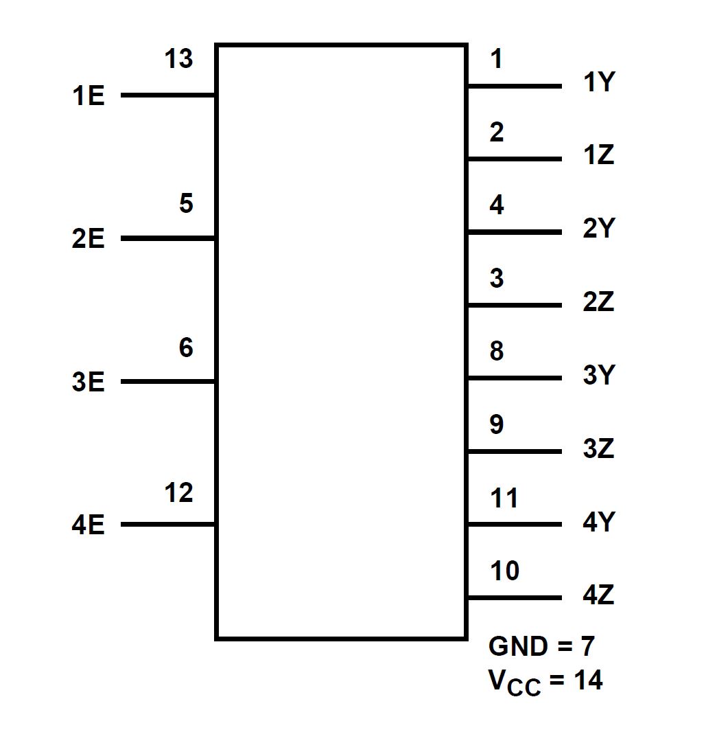 Functional Block
Diagram
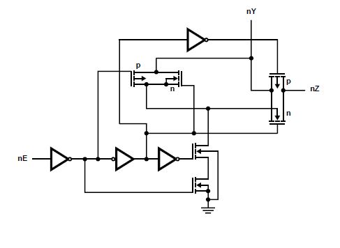 Logic Diagram
 4 Pin Configuration and Functions
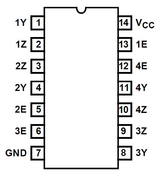 Figure 4-1 CD74HC4066 D or PW Package,
14-Pin SOIC or TSSOP CD74HCT4066 r D Package, 14-Pin SOIC (Top View)
Figure 4-1 CD74HC4066 D or PW Package,
14-Pin SOIC or TSSOP CD74HCT4066 r D Package, 14-Pin SOIC (Top View)| PIN | TYPE(1) | DESCRIPTION | |
|---|---|---|---|
| NAME | NO. | ||
| 1Y | 1 | I/O | Input/Output for Switch 1 |
| 1Z | 2 | I/O | Input/Output for Switch 1 |
| 2Z | 3 | I/O | Input/Output for Switch 2 |
| 2Y | 4 | I/O | Input/Output for Switch 2 |
| 2E | 5 | I | Control pin for Switch 2 |
| 3E | 6 | I | Control pin for Switch 3 |
| GND | 7 | - |
Ground Pin |
| 3Y | 8 | I/O | Input/Output for Switch 3 |
| 3Z | 9 | I/O | Input/Output for Switch 3 |
| 4Z | 10 | I/O | Input/Output for Switch 4 |
| 4Y | 11 | I/O | Input/Output for Switch 4 |
| 4E | 12 | I | Control pin for Switch 4 |
| 1E | 13 | I | Control pin for Switch 1 |
| VCC | 14 | - | Power Pin |
5 Absolute Maximum Ratings
| MIN | MAX | UNIT | |||
|---|---|---|---|---|---|
| VCC HCT | DC Supply voltage | –0.5 | 7 | V | |
| VCC HC(1) | -0.5 | 10.5 | V | ||
| IIK | DC input diode current | For VI < -0.5V or VI > VCC + 0.5V | –20 | 20 | mA |
| IO | DC switch current(2) | For VI< -0.5V or VI > VCC + 0.5V | -20 | 20 | mA |
| IOK | DC Output diode current | For VO < -0.5V or VO > VCC + -0.5V | -25 | 25 | mA |
| DC Output Source or Sink Current per Output Pin, IO | For VO > -0.5V or VO < VCC + -0.5V | –25 | 25 | mA | |
| ICC | DC VCC or ground current | –50 | 50 | mA | |
| TJMAX | Maximum junction temperature (Plastic Package) | 150 | °C | ||
6 ESD Ratings
| VALUE | UNIT | |||
|---|---|---|---|---|
| V(ESD) | Electrostatic discharge | Human body model (HBM), per ANSI/ESDA/JEDEC JS-001, all pins(1) | ±500 | V |
| Charged device model (CDM), per JEDEC specification JESD22-C101, all pins(2) | ±200 | |||
7 Thermal Information
| THERMAL METRIC | CD74HCx4066 | UNIT | |||
|---|---|---|---|---|---|
| D (SOIC) | PW (TSSOP) | ||||
| 14 PINS | 14 PINS | ||||
| RθJA | Junction-to-ambient thermal resistance | 108.4 | 133.9 | °C/W | |
8 Recommended Operating Conditions
| MIN | NOM | MAX | UNIT | |||
|---|---|---|---|---|---|---|
| VCC | Supply voltage range (TA = full package temperature range)(2) | CD54 and 74HC types | 2 | 10 | V | |
| CD54 and 74HCT types | 4.5 | 5.5 | ||||
| VIS | Analog switch I/O voltage | 0 | VCC | V | ||
| TA | Ambient temperature | –55 | 125 | °C | ||
| tr , tf | Input rise and fall times | 2 V | 0 | 1000 | ns | |
| 4.5 V | 0 | 500 | ||||
| 6 V | 0 | 400 | ||||
9 Electrical Characteristics: HC Devices
Over operating free-air temperature range, VSUPPLY = ±5 V, and RL = 100 Ω, (unless otherwise noted)(1)
| PARAMETER | TEST CONDITIONS | MIN | TYP | MAX | UNIT | |||||
|---|---|---|---|---|---|---|---|---|---|---|
| SIGNAL INPUTS (VIS) AND OUTPUTS (VOS) | ||||||||||
| VIS (V) | VI (V) | VCC (V) | TA | |||||||
| High Level Input Voltage | VIH | 2 | 25°C | 1.5 | V | |||||
| –40°C to +85°C | 1.5 | |||||||||
| –55°C to +125°C | 1.5 | |||||||||
| 4.5 | 25°C | 3.15 | ||||||||
| –40°C to +85°C | 3.15 | |||||||||
| –55°C to +125°C | 3.15 | |||||||||
| 9 | 25°C | 6.3 | ||||||||
| –40°C to +85°C | 6.3 | |||||||||
| –55°C to +125°C | 6.3 | |||||||||
| Low Level Input Voltage | VIL | 2 | 25°C | 0.5 | V | |||||
| –40°C to +85°C | 0.5 | |||||||||
| –55°C to +125°C | 0.5 | |||||||||
| 4.5 | 25°C | 1.35 | ||||||||
| –40°C to +85°C | 1.35 | |||||||||
| –55°C to +125°C | 1.35 | |||||||||
| 9 | 25°C | 2.7 | ||||||||
| –40°C to +85°C | 2.7 | |||||||||
| –55°C to +125°C | 2.7 | |||||||||
| "ON" Resistance IO = 1mA | RON | VCC or GND | VCC | 4.5 | 25°C | 25 | 80 | Ω | ||
| –40°C to +85°C | 106 | |||||||||
| –55°C to +125°C | 128 | |||||||||
| 6 | 25°C | 20 | 75 | |||||||
| –40°C to +85°C | 94 | |||||||||
| –55°C to +125°C | 113 | |||||||||
| 9 | 25°C | 15 | 60 | |||||||
| –40°C to +85°C | 78 | |||||||||
| –55°C to +125°C | 95 | |||||||||
| VCC to GND | 4.5 | 25°C | 35 | 95 | Ω | |||||
| –40°C to +85°C | 118 | |||||||||
| –55°C to +125°C | 142 | |||||||||
| 6 | 25°C | 24 | 84 | |||||||
| –40°C to +85°C | 105 | |||||||||
| –55°C to +125°C | 126 | |||||||||
| 9 | 25°C | 31 | 70 | |||||||
| –40°C to +85°C | 88 | |||||||||
| –55°C to +125°C | 105 | |||||||||
| "ON" Resistance Between Any Two Switches | ▲RON | VCC | 4.5 | 25°C | 1 | Ω |
||||
| VCC | 6 | 25°C | 0.75 | |||||||
| VCC | 9 | 25°C | 0.5 | |||||||
| Off-Switch Leakage Current | IZ | VCC or GND | VIL | 10 | 25°C |
±0.1 | µA | |||
| –55°C to 85°C | ±1 | |||||||||
| –55°C to 125°C | ±1 | |||||||||
| Input Leakage Current (Any Control) | IIL | VCC or GND | 10 | 25°C |
±0.1 | µA | ||||
| –55°C to 85°C | ±1 | |||||||||
| –55°C to 125°C | ±1 | |||||||||
Quiescent Device Current |
ICC | VCC or GND | 6 | 25°C |
18.5 | µA | ||||
| –55°C to 85°C | 20 | |||||||||
| –55°C to 125°C | 40 | |||||||||
| 10 | 25°C |
35 | ||||||||
| –55°C to 85°C | 160 | |||||||||
| –55°C to 125°C | 320 | |||||||||
| CONTROL (ADDRESS OR INHIBIT), VC | ||||||||||
10 Electrical Characteristics: HCT Devices
Over operating free-air temperature range, VSUPPLY = ±5 V, and RL = 100 Ω, (unless otherwise noted)(1)
| PARAMETER | TEST CONDITIONS | MIN | TYP | MAX | UNIT | |||||
|---|---|---|---|---|---|---|---|---|---|---|
| SIGNAL INPUTS (VIS) AND OUTPUTS (VOS) | ||||||||||
| VIS (V) | VI (V) | VCC (V) | TA | |||||||
| High Level Input Voltage | VIH | 4.5 to 5.5 | 25°C | 2 | V | |||||
| –40°C to +85°C | 2 | |||||||||
| –55°C to +125°C | 2 | |||||||||
| Low Level Input Voltage | VIL | 25°C | 0.8 | V | ||||||
| –40°C to +85°C | 0.8 | |||||||||
| –55°C to +125°C | 0.8 | |||||||||
| "ON" Resistance IO = 1mA | RON | VCC or GND | VCC | 4.5 | 25°C | 25 | 80 | Ω | ||
| –40°C to +85°C | 106 | |||||||||
| –55°C to +125°C | 128 | |||||||||
| VCC to GND | 25°C | 35 | 95 | Ω | ||||||
| –40°C to +85°C | 118 | |||||||||
| –55°C to +125°C | 142 | |||||||||
| "ON" Resistance Between Any Two Switches | ▲RON | VCC | 4.5 | 25°C | 1 | Ω |
||||
| Off-Switch Leakage Current | IZ | VCC or GND | VIL | 5.5 | 25°C |
±0.1 | µA | |||
| –55°C to 85°C | ±1 | |||||||||
| –55°C to 125°C | ±1 | |||||||||
| Input Leakage Current (Any Control) | IIL | VCC or GND | 5.5 | 25°C |
±0.1 | µA | ||||
| –55°C to 85°C | ±1 | |||||||||
| –55°C to 125°C | ±1 | |||||||||
Quiescent Device Current |
ICC | VCC or GND | 5.5 | 25°C |
2 | µA | ||||
| –55°C to 85°C | 20 | |||||||||
| –55°C to 125°C | 40 | |||||||||
Additional Quiescent Device Current Per Input Pin: 1 Unit Load |
▲ICC | VCC - 2.1 | 4.5 to 5.5 | 25°C |
100 | 360 | ||||
| –55°C to 85°C | 450 | |||||||||
| –55°C to 125°C | 490 | |||||||||
| CONTROL (ADDRESS OR INHIBIT), VC | ||||||||||
11 Switching Characteristics HC
| Parameter | Test Conditions | CL (pF) | MIN | NOM | MAX | UNIT | ||
|---|---|---|---|---|---|---|---|---|
| Propagation Delay Time Switch In to Out | tPHL, tPLH | 2 |
25°C | 50 | 60 | ns | ||
| -40°C to 85°C | 75 | ns | ||||||
| -55°C to 125°C | 90 | ns | ||||||
| 4.5 | 25°C | 12 | ns | |||||
| -40°C to 85°C | 15 | ns | ||||||
| -55°C to 125°C | 18 | ns | ||||||
| 9 | 25°C | 8 | ns | |||||
| -40°C to 85°C | 11 | ns | ||||||
| -55°C to 125°C | 13 | ns | ||||||
| 5 | 25°C | 15 | 4 | ns | ||||
| Propagation Delay Time Switch Turn On Delay | tPZH, tPZL | 2 | 25°C | 50 | 100 | ns | ||
| -40°C to 85°C | 125 | ns | ||||||
| -55°C to 125°C | 150 | ns | ||||||
| 4.5 | 25°C | 20 | ns | |||||
| -40°C to 85°C | 25 | ns | ||||||
| -55°C to 125°C | 30 | ns | ||||||
| 9 | 25°C | 12 | ns | |||||
| -40°C to 85°C | 15 | ns | ||||||
| -55°C to 125°C | 18 | ns | ||||||
| 5 | 25°C | 15 | 4 | ns | ||||
| Propagation Delay Time Switch Turn Off Delay | tPHZ, tPLZ | 2 | 25°C | 50 | 150 | ns | ||
| -40°C to 85°C | 190 | ns | ||||||
| -55°C to 125°C | 225 | ns | ||||||
| 4.5 | 25°C | 30 | ns | |||||
| -40°C to 85°C | 38 | ns | ||||||
| -55°C to 125°C | 45 | ns | ||||||
| 9 | 25°C | 24 | ns | |||||
| -40°C to 85°C | 30 | ns | ||||||
| -55°C to 125°C | 36 | ns | ||||||
| 5 | 25°C | 15 | 9.5 | ns | ||||
| Input (Control) Capacitance | CI | 25°C | 10 | pF | ||||
| -40°C to 85°C | 10 | |||||||
| -55°C to 125°C | 10 | |||||||
| CPD Power dissipation capacitance(1) | CPD | 5 | 25°C | 25 | ||||
12 Switching Characteristics HCT
| Parameter | Test Conditions | CL (pF) | MIN | NOM | MAX | UNIT | ||
|---|---|---|---|---|---|---|---|---|
| Propagation Delay Time Switch In to Out | tPHL, tPLH | 4.5 | 25°C | 50 | 12 | ns | ||
| -40°C to 85°C | 15 | ns | ||||||
| -55°C to 125°C | 18 | ns | ||||||
| 5 | 25°C | 15 | 1.3 | ns | ||||
| Propagation Delay Time Switch Turn On Delay | tPZH, tPZL | 4.5 | 25°C | 50 | 24 | ns | ||
| -40°C to 85°C | 30 | ns | ||||||
| -55°C to 125°C | 36 | ns | ||||||
| 5 | 25°C | 15 | 5 | ns | ||||
| Propagation Delay Time Switch Turn Off Delay | tPHZ, tPLZ | 4.5 | 25°C | 50 | 35 | ns | ||
| -40°C to 85°C | 44 | ns | ||||||
| -55°C to 125°C | 53 | ns | ||||||
| 5 | 25°C | 15 | 5.5 | ns | ||||
| Input (Control) Capacitance | CI | 25°C | 10 | pF | ||||
| -40°C to 85°C | 10 | |||||||
| -55°C to 125°C | 10 | |||||||
| CPD Power dissipation capacitance(1) | CPD | 5 | 25°C | 38 | ||||
13 Analog Channel Specifications
| Parameter | Test Conditions | VCC (V) | HC | HCT | UNIT | ||
|---|---|---|---|---|---|---|---|
| Switch Frequency Response Bandwidth at -3dB | 4.5 | 200 | 200 | MHz | |||
| Cross Talk Between Any Two Switches | 4.5 | -72 | -72 | dB | |||
| Total Harmonic Distortion | 1kHz, VIS= 4VPP | 4.5 | 0.022 | 0.023 | % | ||
| 1kHz, VIS= 8VPP | 9 | 0.019 | N/A | % | |||
| Control to Switch Feedthrough Noise | Control to Switch Feedthrough Noise | 4.5 | 200 | 130 | mV | ||
| Control to Switch Feedthrough Noise | 4.5 | 200 | 130 | mV | |||
| 9 | 550 | N/A | |||||
| Switch "OFF" signal feedthrough | 4.5 | -72 | -72 | dB | |||
| CI Switch input capacitance |
5 | 5 | pF | ||||
14 Analog Test Circuits
 Figure 14-1 Crosstalk
Between Two Switches Test Circuit
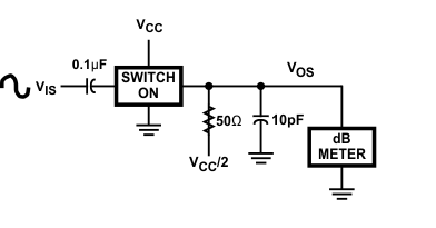 Figure 14-2 Frequency Response Test Circuit
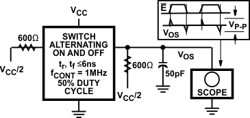 Figure 14-4 Control-To-Switch Feedthrough Noise Test Circuit
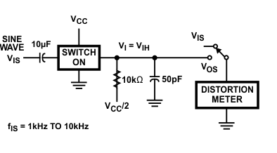 Figure 14-3 Total
Harmonic Distortion Test Circuit
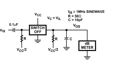 Figure 14-5 Switch OFF Signal Feedthrough
15 Test Circuits and Waveforms
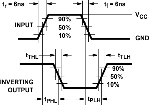 Figure 15-1 HC
Transition Times and Propagation Delay Times, Combination Logic
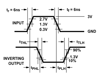 Figure 15-2 HCT
Transition Times and Propagation Delay Times, Combination Logic
Figure 15-2 HCT
Transition Times and Propagation Delay Times, Combination Logic16 Detailed Description
16.1 Functional Block Diagram
 Figure 16-1 Functional Block
Diagram
 Figure 16-2 Logic Diagram
17 Device and Documentation Support
TI offers an extensive line of development tools. Tools and software to evaluate the performance of the device, generate code, and develop solutions are listed below.
17.1 Receiving Notification of Documentation Updates
To receive notification of documentation updates, navigate to the device product folder on ti.com. Click on Notifications to register and receive a weekly digest of any product information that has changed. For change details, review the revision history included in any revised document.
17.2 Support Resources
TI E2E™ support forums are an engineer's go-to source for fast, verified answers and design help — straight from the experts. Search existing answers or ask your own question to get the quick design help you need.
Linked content is provided "AS IS" by the respective contributors. They do not constitute TI specifications and do not necessarily reflect TI's views; see TI's Terms of Use.
17.3 Trademarks
TI E2E™ is a trademark of Texas Instruments.
All trademarks are the property of their respective owners.
17.4 Electrostatic Discharge Caution
 |
This integrated circuit can be damaged by ESD. Texas Instruments recommends that all integrated circuits be handled with appropriate precautions. Failure to observe proper handling and installation procedures can cause damage. |
| ESD damage can range from subtle performance degradation to complete device failure. Precision integrated circuits may be more susceptible to damage because very small parametric changes could cause the device not to meet its published specifications. |
17.5 Glossary
-
TI Glossary
This glossary lists and explains terms, acronyms, and definitions.
18 Revision History
Changes from Revision D (August 2003) to Revision E (July 2024)
19 Mechanical, Packaging, and Orderable Information
The following pages include mechanical, packaging, and orderable information. This information is the most current data available for the designated devices. This data is subject to change without notice and revision of this document. For browser-based versions of this data sheet, refer to the left-hand navigation.
IMPORTANT NOTICE AND DISCLAIMER
TI PROVIDES TECHNICAL AND RELIABILITY DATA (INCLUDING DATASHEETS), DESIGN RESOURCES (INCLUDING REFERENCE DESIGNS), APPLICATION OR OTHER DESIGN ADVICE, WEB TOOLS, SAFETY INFORMATION, AND OTHER RESOURCES “AS IS” AND WITH ALL FAULTS, AND DISCLAIMS ALL WARRANTIES, EXPRESS AND IMPLIED, INCLUDING WITHOUT LIMITATION ANY IMPLIED WARRANTIES OF MERCHANTABILITY, FITNESS FOR A PARTICULAR PURPOSE OR NON-INFRINGEMENT OF THIRD PARTY INTELLECTUAL PROPERTY RIGHTS.
These resources are intended for skilled developers designing with TI products. You are solely responsible for (1) selecting the appropriate TI products for your application, (2) designing, validating and testing your application, and (3) ensuring your application meets applicable standards, and any other safety, security, or other requirements. These resources are subject to change without notice. TI grants you permission to use these resources only for development of an application that uses the TI products described in the resource. Other reproduction and display of these resources is prohibited. No license is granted to any other TI intellectual property right or to any third party intellectual property right. TI disclaims responsibility for, and you will fully indemnify TI and its representatives against, any claims, damages, costs, losses, and liabilities arising out of your use of these resources.
TI’s products are provided subject to TI’s Terms of Sale (www.ti.com/legal/termsofsale.html) or other applicable terms available either on ti.com or provided in conjunction with such TI products. TI’s provision of these resources does not expand or otherwise alter TI’s applicable warranties or warranty disclaimers for TI products.
Mailing Address: Texas Instruments, Post Office Box 655303, Dallas, Texas 75265
Copyright © 2024, Texas Instruments Incorporated