-
CDCLVP1204 Four LVPECL Output, High-Performance Clock Buffer
- 1 Features
- 2 Applications
- 3 Description
- 4 Revision History
- 5 Pin Configuration and Functions
-
6 Specifications
- 6.1 Absolute Maximum Ratings
- 6.2 ESD Ratings
- 6.3 Recommended Operating Conditions
- 6.4 Thermal Information
- 6.5 Terminal Characteristics
- 6.6 Electrical Characteristics: LVCMOS Input
- 6.7 Electrical Characteristics: Differential Input
- 6.8 Electrical Characteristics: LVPECL Output
- 6.9 Electrical Characteristics: LVPECL Output
- 6.10 Timing Diagrams
- 6.11 Typical Characteristics
- 7 Parameter Measurement Information
- 8 Detailed Description
- 9 Applications and Implementation
- 10Power Supply Recommendations
- 11Layout
- 12Device and Documentation Support
- 13Mechanical, Packaging, and Orderable Information
- IMPORTANT NOTICE
Package Options
Mechanical Data (Package|Pins)
- RGT|16
Thermal pad, mechanical data (Package|Pins)
- RGT|16
Orderable Information
CDCLVP1204 Four LVPECL Output, High-Performance Clock Buffer
1 Features
- 2:4 Differential Buffer
- Selectable Clock Inputs Through Control Terminal
- Universal Inputs Accept LVPECL, LVDS, and LVCMOS/LVTTL
- Four LVPECL Outputs
- Maximum Clock Frequency: 2 GHz
- Maximum Core Current Consumption: 45 mA
- Very Low Additive Jitter: <100 fs, RMS in 10-kHz to 20-MHz Offset Range:
- 57 fs, RMS (typical) at 122.88 MHz
- 48 fs, RMS (typical) at 156.25 MHz
- 30 fs, RMS (typical) at 312.5 MHz
- 2.375-V to 3.6-V Device Power Supply
- Maximum Propagation Delay: 450 ps
- Maximum Output Skew: 15 ps
- LVPECL Reference Voltage, VAC_REF, Available for Capacitive-Coupled Inputs
- Industrial Temperature Range: –40°C to +85°C
- Supports 105°C PCB Temperature (Measured at Thermal Pad)
- ESD Protection Exceeds 2 kV (HBM)
2 Applications
- Wireless Communications
- Telecommunications/Networking
- Medical Imaging
- Test and Measurement Equipment
3 Description
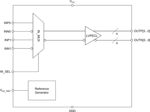
The CDCLVP1204 is a highly versatile, low additive jitter buffer that can generate four copies of LVPECL clock outputs from one of two selectable LVPECL, LVDS, or LVCMOS inputs for a variety of communication applications. It has a maximum clock frequency up to 2 GHz. The CDCLVP1204 features an on-chip multiplexer (MUX) for selecting one of two inputs that can be easily configured solely through a control terminal. The overall additive jitter performance is less than 0.1 ps, RMS from 10 kHz to 20 MHz, and overall output skew is as low as 15 ps, making the device a perfect choice for use in demanding applications.
The CDCLVP1204 clock buffer distributes one of two selectable clock inputs (IN0, IN1) to four pairs of differential LVPECL clock outputs (OUT0, OUT3) with minimum skew for clock distribution. The CDCLVP1204 can accept two clock sources into an input multiplexer. The inputs can be LVPECL, LVDS, or LVCMOS/LVTTL.
The CDCLVP1204 is specifically designed for driving 50-Ω transmission lines. When driving the inputs in single-ended mode, the LVPECL bias voltage (VAC_REF) must be applied to the unused negative input terminal. However, for high-speed performance up to 2 GHz, differential mode is strongly recommended.
The CDCLVP1204 is characterized for operation from –40°C to +85°C.
Device Information(1)
| PART NUMBER | PACKAGE | BODY SIZE (NOM) |
|---|---|---|
| CDCLVP1204 | QFN (16) | 3.00 mm × 3.00 mm |
- For all available packages, see the orderable addendum at the end of the data sheet.
Simplified Schematic

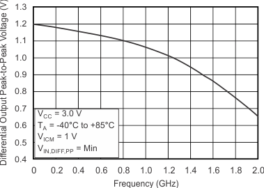
Differential Output Peak-to-Peak Voltage
vs. Frequency

4 Revision History
Changes from E Revision (September 2014) to F Revision
- Deleted Device Comparison Table; same information in POA Go
- Added Support for 105ºC thermal pad temperature Go
- Changed Handing Ratings to ESD Ratings (format update). Go
- Added added PCB temperature in Recommended Operating ConditionsGo
- Added VOH specification for TPCB≤ 105ºC in Electrical Characteristics: LVPECL Output, at VCC = 2.375 V to 2.625 VGo
- Added VOL specification for TPCB≤ 105ºC in Electrical Characteristics: LVPECL Output, at VCC = 2.375 V to 2.625 VGo
- Added IEE specification for TPCB ≤ 105ºC in Electrical Characteristics: LVPECL Output, at VCC = 2.375 V to 2.625 VGo
- Added ICC specification for TPCB ≤ 105ºC in Electrical Characteristics: LVPECL Output, at VCC = 2.375 V to 2.625 V Go
- Added VOH specification for TPCB≤ 105ºC in Electrical Characteristics: LVPECL Output, at VCC = 3 V to 3.6 VGo
- Added VOL specification for TPCB≤ 105ºC in Electrical Characteristics: LVPECL Output, at VCC = 3 V to 3.6 VGo
- Added IEE specification for TPCB ≤ 105ºC in Electrical Characteristics: LVPECL Output, at VCC = 3 V to 3.6 V Go
- Added ICC specification for TPCB ≤ 105ºC in Electrical Characteristics: LVPECL Output, at VCC = 3 V to 3.6 VGo
- Added Thermal Considerations section Go
Changes from D Revision (June 2014) to E Revision
- Changed JEDEC symbol from θJA to RθJAGo
- Added NOTE at the beginning of Applications and Implementation section.Go
Changes from C Revision (August 2011) to D Revision
- Added data sheet flow and layout to conform with new TI standards. Added the following sections: Application and Implementation; Power Supply Recommendations; Layout; Device and Documentation Support; Mechanical, Packaging, and Ordering InformationGo
- Added fIN = 125 MHz, 312.5 MHz for VOUT, DIFF, PPGo
- Added Typical values, Max values, and footnotes for 122.88 MHz, 156.25 MHz, and 312.5 MHz test conditions corresponding to Random Additive Jitter in Electrical Characteristics: LVPECL Output, at VCC = 2.375 V to 2.625 VGo
- Added Typical values, Max values, and footnotes for 122.88 MHz, 156.25 MHz, and 312.5 MHz test conditions corresponding to Random Additive Jitter in Electrical Characteristics: LVPECL Output, at VCC = 3.0 V to 3.6 VGo
Changes from B Revision (May, 2010) to C Revision
- Revised description of pin 8Go
- Corrected VIL parameter description in Electrical Characteristics table for LVCMOS inputsGo
- Added footnote (2) to Electrical Characteristics table for LVPECL Output, VCC = 2.375 V to 2.625 VGo
- Changed recommended resistor values in Figure 12(a)Go
- Changed recommended resistor values in Figure 16Go
- Changed recommended resistor values in Figure 17Go
Changes from A Revision (October, 2009) to B Revision
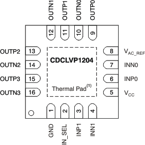
5 Pin Configuration and Functions

Pin Functions
| PIN | TYPE | DESCRIPTION | |
|---|---|---|---|
| NAME | NUMBER | ||
| VCC | 5 | Power | 3.3-V supply for the device |
| GND | 1 | Ground | Device ground |
| INP0, INN0 | 6, 7 | Input | Differential input pair or single-ended input. Unused input pair can be left floating. |
| INP1, INN1 | 3, 4 | Input | Redundant differential input pair or single-ended input. Unused input pair can be left floating. |
| OUTP3, OUTN3 | 15, 16 | Output | Differential LVPECL output pair no. 3. Unused output pair can be left floating. |
| OUTP2, OUTN2 | 13, 14 | Output | Differential LVPECL output pair no. 2. Unused output pair can be left floating. |
| OUTP1, OUTN1 | 11, 12 | Output | Differential LVPECL output pair no. 1. Unused output pair can be left floating. |
| OUTP0 OUTN0 | 9, 10 | Output | Differential LVPECL output pair no. 0. Unused output pair can be left floating. |
| VAC_REF | 8 | — | Bias voltage output for capacitive-coupled inputs. Do not use VAC_REF at VCC < 3 V. If used, it is recommended to use a 0.1-μF capacitor to GND on this pin. The output current is limited to 2 mA. |
| IN_SEL | 2 | — | Pulldown (see Terminal Characteristics) MUX select input for input choice (see Table 1) |
Table 1. Input Selection Table
| IN_SEL | ACTIVE CLOCK INPUT |
|---|---|
| 0 | INP0, INN0 |
| 1 | INP1, INN1 |
6 Specifications
6.1 Absolute Maximum Ratings
over operating free-air temperature range (unless otherwise noted) (1)| MIN | MAX | UNIT | ||
|---|---|---|---|---|
| VCC | Supply voltage range(2) | –0.5 | 4.6 | V |
| VIN | Input voltage range(3) | –0.5 | VCC + 0.5 | V |
| VOUT | Output voltage range(3) | –0.5 | VCC + 0.5 | V |
| IIN | Input current | 20 | mA | |
| IOUT | Output current | 50 | mA | |
| TA | Specified free-air temperature range (no airflow) | –40 | 85 | °C |
| TJ | Maximum junction temperature | 125 | °C | |
| Tstg | Storage temperature | –65 | 150 | °C |
6.2 ESD Ratings
| VALUE | UNIT | |||
|---|---|---|---|---|
| V(ESD) | Electrostatic discharge | Human-body model (HBM), per ANSI/ESDA/JEDEC JS-001(1) | ±2000 | V |
6.3 Recommended Operating Conditions
Over operating free-air temperature range (unless otherwise noted).| MIN | NOM | MAX | UNIT | |||
|---|---|---|---|---|---|---|
| VCC | Supply voltage | 2.375 | 2.50/3.30 | 3.60 | V | |
| TA | Ambient temperature | –40 | 85 | °C | ||
| TPCB | PCB temperature (measured at thermal pad) | 105 | °C | |||
6.4 Thermal Information
| THERMAL METRIC(1)(3)(4) | CDCLVP1204 | UNIT | |
|---|---|---|---|
| RGT (QFN) | |||
| 16 PINS | |||
| RθJA | Junction-to-ambient thermal resistance | 51.8, 0 LFM(2) | °C/W |
| 22.6, 150 LFM(2) | |||
| 19.2, 400 LFM(2) | |||
| RθJC(top) | Junction-to-case (top) thermal resistance | 79 | °C/W |
| RθJP(5) | Junction-to-pad thermal resistance | 6.12(2) | °C/W |
| ψJT | Junction-to-top characterization parameter | 1.4 | °C/W |
| ψJB | Junction-to-board characterization parameter | 19 | °C/W |
| RθJC(bot) | Junction-to-case (bottom) thermal resistance | 6.12 | °C/W |
6.5 Terminal Characteristics
| PARAMETER | MIN | TYP | MAX | UNIT | |
|---|---|---|---|---|---|
| RPULLDOWN | Input pulldown resistor | 150 | kΩ | ||
6.6 Electrical Characteristics: LVCMOS Input
At VCC = 2.375 V to 3.6 V and TA = –40°C to +85°C and TPCB ≤ 105°C (unless otherwise noted).(1)6.7 Electrical Characteristics: Differential Input
At VCC = 2.375 V to 3.6 V and TA = –40°C to +85°C and TPCB ≤ 105°C (unless otherwise noted). (1)| PARAMETER | TEST CONDITIONS | MIN | TYP | MAX | UNIT | |
|---|---|---|---|---|---|---|
| fIN | Input frequency | Clock input | 2000 | MHz | ||
| VIN, DIFF, PP | Differential input peak-peak voltage | fIN ≤ 1.5 GHz | 0.1 | 1.5 | V | |
| 1.5 GHz ≤ fIN ≤ 2 GHz | 0.2 | 1.5 | V | |||
| VICM | Input common-mode level | 1 | VCC – 0.3 | V | ||
| IIH | Input high current | VCC = 3.6 V, VIH = 3.6 V | 40 | μA | ||
| IIL | Input low current | VCC = 3.6 V, VIL = 0 V | –40 | μA | ||
| ΔV/ΔT | Input edge rate | 20% to 80% | 1.5 | V/ns | ||
| ICAP | Input capacitance | 5 | pF |
6.8 Electrical Characteristics: LVPECL Output
VCC = 2.375 V to 2.625 V; TA = –40°C to +85°C and TPCB ≤ 105°C (unless otherwise noted).(1)| PARAMETER | TEST CONDITIONS | MIN | TYP | MAX | UNIT | |
|---|---|---|---|---|---|---|
| VOH | Output high voltage | TA ≤ 85ºC | VCC – 1.26 | VCC – 0.9 | V | |
| TPCB ≤ 105ºC | VCC – 1.26 | VCC – 0.83 | V | |||
| VOL | Output low voltage | TA ≤ 85ºC | VCC – 1.7 | VCC – 1.3 | V | |
| TPCB ≤ 105ºC | VCC – 1.7 | VCC – 1.25 | V | |||
| VOUT, DIFF, PP | Differential output peak-peak voltage | fIN ≤ 2 GHz | 0.5 | 1.35 | V | |
| fIN = 125 MHz, 312.5 MHz | 1.15 | |||||
| VAC_REF | Input bias voltage(2) | IAC_REF = 2 mA | VCC – 1.6 | VCC – 1.1 | V | |
| tPD | Propagation delay | VIN, DIFF, PP = 0.1 V | 450 | ps | ||
| VIN, DIFF, PP = 0.3 V | 450 | ps | ||||
| tSK,PP | Part-to-part skew | 100 | ps | |||
| tSK,O | Output skew | 15 | ps | |||
| tSK,P | Pulse skew (with 50% duty cycle input) | Crossing-point-to-crossing-point distortion, fOUT = 100 MHz |
–50 | 50 | ps | |
| tRJIT | Random additive jitter (with 50% duty cycle input) |
fOUT = 100 MHz, VIN,SE = VCC, Vth = 1.25 V, 10 kHz to 20 MHz |
0.081 | ps, RMS | ||
| fOUT = 100 MHz, VIN,SE = 0.9 V, Vth = 1.1 V, 10 kHz to 20 MHz |
0.091 | ps, RMS | ||||
| fOUT = 2 GHz, VIN,DIFF,PP = 0.2 V, VICM = 1 V, 10 kHz to 20 MHz |
0.041 | ps, RMS | ||||
| fOUT = 100 MHz, VIN,DIFF,PP = 0.15 V, VICM = 1 V, 10 kHz to 20 MHz |
0.088 | ps, RMS | ||||
| fOUT = 100 MHz, VIN,DIFF,PP = 1 V, VICM = 1 V, 10 kHz to 20 MHz |
0.081 | ps, RMS | ||||
| fOUT = 122.88 MHz,(6)(3)
Square Wave, VIN-PP = 1 V, 12 kHz to 20 MHz |
0.057 | 0.088 | ps, RMS | |||
| fOUT = 122.88 MHz,(6)(3)
Square Wave, VIN-PP = 1 V, 10 kHz to 20 MHz |
0.057 | 0.088 | ps, RMS | |||
| fOUT = 122.88 MHz,(6)(3)
Square Wave, VIN-PP = 1 V, 1 kHz to 40 MHz |
0.086 | 0.121 | ps, RMS | |||
| fOUT = 156.25 MHz,(6)(4)
Square Wave, VIN-PP = 1 V, 12 kHz to 20 MHz |
0.048 | 0.071 | ps, RMS | |||
| fOUT = 156.25 MHz,(6)(4)
Square Wave, VIN-PP = 1 V, 10 kHz to 20 MHz |
0.048 | 0.071 | ps, RMS | |||
| fOUT = 156.25 MHz,(6)(4)
Square Wave, VIN-PP = 1 V, 1 kHz to 40 MHz |
0.068 | 0.097 | ps, RMS | |||
| fOUT = 312.5 MHz,(6)(5)
Square Wave, VIN-PP = 1 V, 12 kHz to 20 MHz |
0.030 | 0.048 | ps, RMS | |||
| fOUT = 312.5 MHz,(6)(5)
Square Wave, VIN-PP = 1 V, 10 kHz to 20 MHz |
0.030 | 0.048 | ps, RMS | |||
| fOUT = 312.5 MHz,(6)(5)
Square Wave, VIN-PP = 1 V, 1 kHz to 40 MHz |
0.045 | 0.068 | ps, RMS | |||
| tR/tF | Output rise/fall time | 20% to 80% | 200 | ps | ||
| IEE | Supply internal current | Outputs unterminated TA ≤ 85ºC |
45 | mA | ||
| Outputs unterminated, TPCB ≤ 105ºC |
47 | mA | ||||
| ICC | Output and internal supply current | All outputs terminated, 50 Ω to VCC – 2 TA ≤ 85ºC |
170 | mA | ||
| All outputs terminated, 50 Ω to VCC – 2 TPCB ≤ 105ºC |
186 | mA | ||||
6.9 Electrical Characteristics: LVPECL Output
VCC = 3 V to 3.6 V; TA = –40°C to +85°C and TPCB ≤ 105°C (unless otherwise noted).(1)| PARAMETER | TEST CONDITIONS | MIN | TYP | MAX | UNIT | |
|---|---|---|---|---|---|---|
| VOH | Output high voltage | TA ≤ 85ºC | VCC – 1.26 | VCC – 0.9 | V | |
| TPCB ≤ 105ºC | VCC – 1.26 | VCC – 0.85 | V | |||
| VOL | Output low voltage | TA ≤ 85ºC | VCC – 1.7 | VCC – 1.3 | V | |
| TPCB ≤ 105ºC | VCC – 1.7 | VCC – 1.3 | V | |||
| VOUT, DIFF, PP | Differential output peak-peak voltage | fIN ≤ 2 GHz | 0.65 | 1.35 | V | |
| VAC_REF | Input bias voltage | IAC_REF = 2 mA | VCC – 1.6 | VCC – 1.1 | V | |
| tPD | Propagation delay | VIN, DIFF, PP = 0.1 V | 450 | ps | ||
| VIN, DIFF, PP = 0.3 V | 450 | ps | ||||
| tSK,PP | Part-to-part skew | 100 | ps | |||
| tSK,O | Output skew | 15 | ps | |||
| tSK,P | Pulse skew (with 50% duty cycle input) | Crossing-point-to-crossing-point distortion, fOUT = 100 MHz |
–50 | 50 | ps | |
| tRJIT | Random additive jitter (with 50% duty cycle input) fOUT = 100 MHz(6) |
fOUT = 100 MHz, VIN,SE = VCC, Vth = 1.65 V, 10 kHz to 20 MHz |
0.079 | ps, RMS | ||
| fOUT = 100 MHz, VIN,SE = 0.9 V, Vth = 1.1 V, 10 kHz to 20 MHz |
0.097 | ps, RMS | ||||
| fOUT = 2 GHz, VIN,DIFF,PP = 0.2 V, VICM = 1 V, 10 kHz to 20 MHz |
0.058 | ps, RMS | ||||
| fOUT = 100 MHz, VIN,DIFF,PP = 0.15 V, VICM = 1 V, 10 kHz to 20 MHz |
0.094 | ps, RMS | ||||
| fOUT = 100 MHz, VIN,DIFF,PP = 1 V, VICM = 1 V, 10 kHz to 20 MHz |
0.088 | ps, RMS | ||||
| fOUT = 100 MHz, Input AC coupled, VICM = VAC_REF, 12 kHz to 20 MHz |
0.068 | ps, RMS | ||||
| Random additive jitter (with 50% duty cycle input) fOUT = 122.88 MHz(6) |
fOUT = 122.88 MHz,(2)(5)
Square Wave, VIN-PP = 1 V, 12 kHz to 20 MHz |
0.057 | ps, RMS | |||
| fOUT = 122.88 MHz,(2)(5)
Square Wave, VIN-PP = 1 V, 10 kHz to 20 MHz |
0.057 | ps, RMS | ||||
| fOUT= 122.88 MHz,(2)(5)
Square Wave, VIN-PP = 1 V, 1 kHz to 40 MHz |
0.086 | ps, RMS | ||||
| tRJIT | Random additive jitter (with 50% duty cycle input) fOUT = 156.25 MHz(6) |
fOUT = 156.25 MHz,(5)(3)
Square Wave, VIN-PP = 1 V, 12 kHz to 20 MHz |
0.048 | ps, RMS | ||
| fOUT = 156.25 MHz,(5)(3)
Square Wave, VIN-PP = 1 V, 10 kHz to 20 MHz |
0.048 | ps, RMS | ||||
| fOUT = 156.25 MHz,(5)(3)
Square Wave, VIN-PP = 1 V, 1 kHz to 40 MHz |
0.068 | ps, RMS | ||||
| Random additive jitter (with 50% duty cycle input) fOUT = 312.5 MHz(6) |
fOUT = 312.5 MHz,(5)(4)
Square Wave, VIN-PP = 1 V, 12 kHz to 20 MHz |
0.030 | ps, RMS | |||
| fOUT = 312.5 MHz,(5)(4)
Square Wave, VIN-PP = 1 V, 10 kHz to 20 MHz |
0.030 | ps, RMS | ||||
| fOUT = 312.5 MHz,(5)(4)
Square Wave, VIN-PP = 1 V, 1 kHz to 40 MHz |
0.045 | ps, RMS | ||||
| tR/tF | Output rise/fall time | 20% to 80% | 200 | ps | ||
| IEE | Supply internal current | Outputs unterminated TA ≤ 85ºC |
45 | mA | ||
| Outputs unterminated, TPCB ≤ 105ºC |
47 | mA | ||||
| ICC | Output and internal supply current | All outputs terminated, 50 Ω to VCC – 2 TA ≤ 85ºC |
170 | mA | ||
| All outputs terminated, 50 Ω to VCC – 2 TPCB ≤ 105ºC |
186 | mA | ||||
6.10 Timing Diagrams
 Figure 1. Output Voltage and Rise/Fall Time

6.11 Typical Characteristics
At TA = –40°C to +85°C (unless otherwise noted).

7 Parameter Measurement Information
7.1 Test Configurations
Figure 5 through Figure 11 illustrate how the device must be set up for a variety of test configurations for each block for the CDCLVP1204.
 Figure 5. DC-Coupled LVPECL Input During Device Test
 Figure 6. DC-Coupled LVCMOS Input During Device Test
 Figure 7. Voltage Variation Over LVCMOS Vth Levels
 Figure 8. DC-Coupled LVDS Input During Device Test
 Figure 9. AC-Coupled Differential Input To Device
 Figure 10. LVPECL Output DC Configuration During Device Test
 Figure 11. LVPECL Output AC Configuration During Device Test