LMG2610 用于有源钳位反激式转换器的集成 650V GaN 半桥
1 特性
- 650V GaN 功率 FET 半桥
- 170mΩ 低侧和 248mΩ 高侧 GaN FET
- 具有低传播延迟和可调节导通压摆率控制的集成栅极驱动器
- 具有高带宽和高精度的电流检测仿真
- 低侧/高侧栅极驱动互锁
- 高侧栅极驱动信号电平转换器
- 智能开关自举二极管功能
- 高侧启动:< 8us
- 低侧/高侧逐周期过流保护
- 通过 FLT 引脚报告实现过热保护
- AUX 空闲静态电流:240μA
- AUX 待机静态电流:50μA
- BST 空闲静态电流:60μA
- 最大电源和输入逻辑引脚电压:26V
- 具有双散热焊盘的 9mm x 7mm QFN 封装
2 应用
- 有源钳位反激式电源转换器
- 交流/直流适配器和充电器
- 交流/直流 USB 墙壁插座电源
- 交流/直流辅助电源
简化版方框图
3 说明
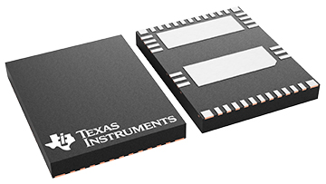
LMG2610 是一款 650V GaN 功率 FET 半桥,适用于开关模式电源应用中 < 75W 的有源钳位反激式 (ACF) 转换器。LMG2610 通过在 9mm x 7mm QFN 封装中集成半桥功率 FET、栅极驱动器、自举二极管和高侧栅极驱动电平转换器,简化了设计、减少了元件数量并减小了布板空间。
非对称 GaN FET 电阻针对 ACF 工作条件进行了优化。可编程导通压摆率可提供 EMI 和振铃控制。与传统的电流检测电阻相比,低侧电流检测仿真可降低功耗,并允许将低侧散热焊盘连接到冷却 PCB 电源接地。
高侧栅极驱动信号电平转换器消除了外部解决方案中出现的噪声和突发模式功率耗散问题。智能开关 GaN 自举 FET 没有二极管正向压降,可避免高侧电源过充,并且反向恢复电荷为零。
LMG2610 具有低静态电流和快速启动时间,支持转换器轻负载效率要求和突发模式运行。保护特性包括 FET 导通互锁、欠压锁定 (UVLO)、逐周期电流限制和过热关断。
| 器件型号 | 封装 (1) | 封装尺寸(标称值) |
|---|---|---|
| LMG2610 | QFN | 9.00 mm x 7.00 mm |
4 Revision History
Changes from Revision * (October 2022) to Revision A (December 2022)
- 将数据表状态从“预告信息”更改为“量产数据”Go
5 Pin Configuration and Functions
| PIN | TYPE(1) | DESCRIPTION | |
|---|---|---|---|
| NAME | NO. | ||
| NC1 | 1, 13 | NC | Used to anchor QFN package to PCB. Pins must be soldered to PCB landing pads. The PCB landing pads are non-solder mask defined pads and must not be physically connected to any other metal on the PCB. Internally connected to DH. |
| DH | 2-12 | P | High-side GaN FET drain. Internally connected to NC1. |
| SW | 14-16 | P | GaN FET half-bridge switch node between the high-side GaN FET source and low-side GaN FET drain. Internally connected to PADH. |
| NC2 | 17, 21, 37 | NC | Used to anchor QFN package to PCB. Pins must be soldered to PCB landing pads. The PCB landing pads are non-solder mask defined pads and must not be physically connected to any other metal on the PCB. Internally connected to AGND, SL, and PADL. |
| SL | 18-20, 22-27 | P | Low-side GaN FET source. Internally connected to AGND, PADL, and NC2. |
| EN | 28 | I | Enable. Used to toggle between active and standby modes. The standby mode has reduced quiescent current to support converter light load efficiency targets. There is a forward biased ESD diode from EN to AUX so avoid driving EN higher than AUX. |
| INH | 29 | I | High-side gate-drive control input. Referenced to AGND. Signal is level shifted internally to the high-side GaN FET driver. There is a forward biased ESD diode from INH to AUX so avoid driving INH higher than AUX. |
| INL | 30 | I | Low-side gate-drive control input. Referenced to AGND. There is a forward biased ESD diode from INL to AUX so avoid driving INL higher than AUX. |
| AGND | 31 | GND | Low-side analog ground. Internally connected to SL, PADL, and NC2. |
| CS | 32 | O | Current-sense emulation output. Outputs 1 ma/A scaled replica of the low-side GaN FET current. Feed output current into a resistor to create a current sense voltage signal. Reference the resistor to the power supply controller IC local ground. This function replaces the external current-sense resistor that is used in series with the low-side FET. |
| NC3 | 33 | NC | Used to anchor QFN package to PCB. Pin must be soldered to a PCB landing pad. The PCB landing pad is non-solder mask defined pad and must not be physically connected to any other metal on the PCB. Pin not connected internally. |
| FLT | 34 | O | Active-low fault output. Open-drain output that asserts during an over-temperature shut down. |
| AUX | 35 | P | Auxiliary voltage rail. Low-side supply voltage. Connect a local bypass capacitor between AUX and AGND. |
| RDRVL | 36 | I | Low-side drive strength control resistor. Set a resistance between RDRVL and AGND to program the low-side GaN FET turn-on slew rate. |
| BST | 38 | P | Bootstrap voltage rail. High-side supply voltage. The bootstrap diode function between AUX and BST is internally provided. Connect an appropriately sized bootstrap capacitor between BST and SW. Recommend to make the SW connection using NC4 as a pass through connection to PADH (PADH = SW) as explained in the NC4 description. |
| RDRVH | 39 | I | High-side drive strength control resistor. Set a resistance between RDRVH and SW to program the high-side GaN FET turn-on slew rate. Recommend to make the SW connection using NC4 as a pass through connection to PADH (PADH = SW) as explained in the NC4 description. |
| NC4 | 40 | NC | Pin is not functional. Pin is high impedance and referenced to SW. Recommend to connect pin to PADH (PADH = SW) to use as convenient connection for the BST bypass capacitor and the RDRVH resistor. See the example board layout in the Layout Example section. |
| PADH | 41 | TP | High-side thermal pad. Internally connected to SW. All the SW current can be conducted with PADH (PADH = SW). |
| PADL | 42 | TP | Low-side thermal pad. Internally connected to SL, AGND, and NC2. All the SL current can be conducted with PADL (PADL = SL). |
6 Specifications
6.1 Absolute Maximum Ratings
| MIN | MAX | UNIT | |||
|---|---|---|---|---|---|
| VDS(ls) | Low-side drain-source (SW to SL) voltage, FET off | 650 | V | ||
| VDS(surge)(ls) | Low-side drain-source (SW to SL) voltage, surge condition, FET off (2) | 720 | V | ||
| VDS(tr)(surge)(ls) | Low-side drain-source (SW to SL) transient ringing peak voltage, surge condition, FET off (2) | 800 | V | ||
| VDS(hs) | High-side drain source (DH to SW) voltage, FET off | 650 | V | ||
| VDS(surge)(hs) | High-side drain-source (DH to SW) voltage, surge condition, FET off (2) | 720 | V | ||
| VDS(tr)(surge)(hs) | High-side drain-source (DH to SW) transient ringing peak voltage, surge condition, FET off (2) | 800 | V | ||
| Pin voltage | AUX | –0.3 | 30 | V | |
| EN, INL, INH, FLT | –0.3 | VAUX + 0.3 | V | ||
| CS | –0.3 | 5.5 | V | ||
| RDRVL | –0.3 | 4 | V | ||
| Pin voltage to SW | BST | –0.3 | 30 | V | |
| RDRVH | –0.3 | 4 | V | ||
| ID(peak)(ls) | Low-side drain (SW to SL) peak current, FET on | –6.4 | Internally limited | A | |
| IS(peak)(ls) | Low-side source (SL to SW) peak current, FET off | 6.4 | A | ||
| ID(peak)(hs) | High-side drain (DH to SW) peak current, FET on | –4 | Internally limited | A | |
| IS(peak)(hs) | High-side source (SW to DH) peak current, FET off | 4 | A | ||
| Positive sink current | CS | 10 | mA | ||
| FLT (while asserted) | Internally limited | mA | |||
| TJ | Operating junction temperature | –40 | 150 | °C | |
| Tstg | Storage temperature | –65 | 150 | °C | |
6.2 ESD Ratings
| VALUE | UNIT | ||||
|---|---|---|---|---|---|
| V(ESD) | Electrostatic discharge | Human body model (HBM), per ANSI/ESDA/JEDEC JS-001(1) | Pins1 through 16, Pins 38 through 40 | ±1000 | V |
| Pins 17 through 37 | ±2000 | V | |||
| Charged device model (CDM), per ANSI/ESDA/JEDEC JS-002(2) | ±500 | V | |||
6.3 Recommended Operating Conditions
| MIN | NOM | MAX | UNIT | |||
|---|---|---|---|---|---|---|
| Supply voltage | AUX | 10 | 26 | V | ||
| Supply voltage to SW | BST | 7.5 | 26 | V | ||
| Input voltage | EN, INL, INH | 0 | VAUX | V | ||
| Pull-up voltage on open-drain output | FLT | 0 | VAUX | V | ||
| VIH | High-level input voltage | EN, INL, INH | 2.5 | V | ||
| VIL | Low-level input voltage | 0.6 | V | |||
| ID(peak)(ls) | Low-side drain (SW to SL) peak current, FET on | –3.2 | 5.4 | A | ||
| ID(peak)(hs) | High-side drain (DH to SW) peak current, FET on | –2 | 3 | A | ||
| CAUX | AUX to AGND capacitance from external bypass capacitor | 3 x CBST | µF | |||
| CBST_SW | BST to SW capacitance from external bypass capacitor | 0.010 | µF | |||
| RRDRVL | RDRVL to AGND resistance from external slew-rate control resistor to configure below low-side slew rate settings | |||||
| slew rate setting 0 (slowest) | 90 | 120 | open | kΩ | ||
| slew rate setting 1 | 42.5 | 47 | 51.5 | kΩ | ||
| slew rate setting 2 | 20 | 22 | 24 | kΩ | ||
| slew rate setting 3 (fastest) | 0 | 5.6 | 11 | kΩ | ||
| RRDRVH_SW | RDRVH to SW resistance from external slew-rate control resistor to configure below high-side slew rate settings | |||||
| slew rate setting 0 (slowest) | 90 | 120 | open | kΩ | ||
| slew rate setting 1 | 42.5 | 47 | 51.5 | kΩ | ||
| slew rate setting 2 | 20 | 22 | 24 | kΩ | ||
| slew rate setting 3 (fastest) | 0 | 5.6 | 11 | kΩ | ||
6.4 Thermal Information
| THERMAL METRIC(1) | LMG2610 | UNIT | |
|---|---|---|---|
| RRG (VQFN) | |||
| 40 Pins | |||
| RθJA | Junction-to-ambient thermal resistance | 25.3 | °C/W |
| RθJC(bot) | Junction-to-case (bottom) thermal resistance | 1.22 | °C/W |
6.5 Electrical Characteristics
| PARAMETER | TEST CONDITIONS | MIN | TYP | MAX | UNIT | |
|---|---|---|---|---|---|---|
| LOW-SIDE GAN POWER FET | ||||||
| RDS(on)(ls) | Drain-source (SW to SL) on resistance | VINL = 5 V, ID(ls) = 3 A, TJ = 25°C | 170 | mΩ | ||
| VINL = 5 V, ID(ls) = 3 A, TJ = 125°C | 325 | |||||
| VSD(ls) | Source-drain (SL to SW) third-quadrant voltage | SL to SW current = 0.1 A | -1.9 | V | ||
| SL to SW current = 1 A | -2.6 | |||||
| IDSS(ls) | Drain (SW to SL) leakage current | VDS(hs) = 0 V, VDS(ls) = 650 V, TJ = 25 °C | 2 | µA | ||
| VDS(hs) = 0 V, VDS(ls) = 650 V, TJ = 125 °C | 10 | |||||
| QOSS(ls) | Output (SW to SL) charge | VDS(hs) = 0 V, VDS(ls) = 400 V | 19.7 | nC | ||
| COSS(ls) | Output (SW to SL) capacitance | 22 | pF | |||
| EOSS(ls) | Output (SW to SL) capacitance stored energy | 2.32 | µJ | |||
| COSS,er(ls) | Energy related effective output (SW to SL) capacitance | 29 | pF | |||
| COSS,tr(ls) | Time related effective output (SW to SL) capacitance | VDS(hs) = 0 V, VDS(ls) = 0 V to 400 V | 49.2 | pF | ||
| QRR(ls) | Reverse recovery charge | 0 | nC | |||
| HIGH-SIDE GAN POWER FET | ||||||
| RDS(on)(hs) | Drain-source (DH to SW) on resistance | VINH = 5 V, ID(hs) = 1.75 A, TJ = 25°C | 248 | mΩ | ||
| VINH = 5 V, ID(hs) = 1.75 A, TJ = 125°C | 470 | |||||
| VSD(hs) | Source-drain (SW to DH) third-quadrant voltage | SW to DH current = 0.1 A | -2 | V | ||
| SW to DH current = 1 A | -2.7 | |||||
| IDSS(hs) | Drain (DH to SW) leakage current | VDS(ls) = 0 V, VDS(hs) = 650 V, TJ = 25 °C | 1.4 | µA | ||
| VDS(ls) = 0 V, VDS(hs) = 650 V, TJ = 125 °C | 7 | |||||
| QOSS(hs) | Output (DH to SW) charge | VDS(ls) = 0 V, VDS(hs) = 400 V | 15.51 | nC | ||
| COSS(hs) | Output (DH to SW) capacitance | 22.4 | pF | |||
| EOSS(hs) | Output (DH to SW) capacitance stored energy | 2.15 | µJ | |||
| COSS,er(hs) | Energy related effective output (DH to SW) capacitance | 26.9 | pF | |||
| COSS,tr(hs) | Time related effective output (DH to SW) capacitance | VDS(ls) = 0 V, VDS(hs) = 0 V to 400 V | 38.78 | pF | ||
| QRR(hs) | Reverse recovery charge | 0 | nC | |||
| LOW-SIDE OVERCURRENT PROTECTION | ||||||
| IT(OC)(ls) | Overcurrent fault – threshold current | 5.4 | 5.9 | 6.4 | A | |
| HIGH-SIDE OVERCURRENT PROTECTION | ||||||
| IT(OC)(hs) | Overcurrent fault – threshold current | 3 | 3.5 | 4 | A | |
| BOOTSTRAP RECTIFIER | ||||||
| RDS(on) | AUX to BST on resistance | VINL = 5 V, VAUX_BST = 1 V, TJ = 25°C | 8 | Ω | ||
| VINL = 5 V, VAUX_BST = 1 V, TJ = 125°C | 14 | |||||
| AUX to BST current limit | VINL = 5 V, VAUX_BST = 7 V | 210 | 240 | 270 | mA | |
| BST to AUX reverse current blocking threshold | VINL = 5 V | 15 | mA | |||
| CS | ||||||
| Current sense gain (ICS(src) / ID(LS)) | VINL = 5 V, 0 A ≤ ID(ls) < IT(OC)(ls), 0 V ≤ VCS ≤ 2 V | 1 | mA/A | |||
| Current sense input offset current | VINL = 5 V, 0 A ≤ ID(ls) < IT(OC)(ls), 0 V ≤ VCS ≤ 2 V | –50 | 50 | mA | ||
| Initial held output after overcurrent fault occurs while INL remains high | VINL = 5 V, 0 V ≤ VCS ≤ 2 V | 7 | mA | |||
| ICS(src)(OC)(final) | Final held output after overcurrent fault occurs while INL remains high | VINL = 5 V, 0 V ≤ VCS ≤ 2 V | 10 | 12 | 15.5 | mA |
| Output clamp voltage | VINL = 5 V, ID(ls) = 5 A, CS sinking 5 mA from external source | 2.5 | V | |||
| EN, INL, INH | ||||||
| VIT+ | Positive-going input threshold voltage | 1.7 | 2.45 | V | ||
| VIT– | Negative-going input threshold voltage | 0.7 | 1.3 | V | ||
| Input threshold voltage hysteresis | 1 | V | ||||
| Pull-down resistance | 0 V ≤ VPIN ≤ 3 V | 200 | 400 | 600 | kΩ | |
| Pull-down current | VAUX = 26 V; 10 V ≤ VPIN ≤ 26 V | 10 | µA | |||
| OVER-TEMPERATURE PROTECTION | ||||||
| Temperature fault – postive-going threshold temperature | 150 | °C | ||||
| Temperature fault – negative-going threshold temperature | 130 | °C | ||||
| Temperature fault – threshold temperature hysteresis | 20 | °C | ||||
| FLT | ||||||
| Low-level output voltage | FLT sinking 1mA while asserted | 200 | mV | |||
| Off-state current | VFLT = VAUX while de-asserted | 1 | µA | |||
| AUX | ||||||
| VAUX,T+(UVLO) | UVLO – positive-going threshold voltage | 8.9 | 9.3 | 9.7 | V | |
| UVLO – negative-going threshold voltage | 8.6 | 9.0 | 9.4 | V | ||
| UVLO – threshold voltage hysteresis | 250 | mV | ||||
| Standby quiescent current | VEN = 0 V | 50 | 80 | µA | ||
| Quiescent current | 250 | 370 | µA | |||
| VINL = 5 V, ID(ls) = 0 A | 1370 | µA | ||||
| Operating current | VINL = 0 V or 5 V, VDS(ls) = 0 V, fINL = 500 kHz, ID(ls) = 0 A | 3.1 | mA | |||
| BST | ||||||
| VBST_SW,T+(UVLO) | VBST_SW UVLO for FET to turn on – positive-going threshold voltage | 6.7 | 7 | 7.3 | V | |
| VBST_SW UVLO for FET to stay on– negative-going threshold voltage | 4.8 | 5.1 | 5.4 | V | ||
| Quiescent current | 65 | 100 | µA | |||
| VINH = 5 V | 330 | |||||
| Operating current | VINH = 0 V or 5 V, VDS(hs) = 0 V; fINH = 500 kHz | 1.2 | mA | |||
6.6 Switching Characteristics
| PARAMETER | TEST CONDITIONS | MIN | TYP | MAX | UNIT | |
|---|---|---|---|---|---|---|
| LOW-SIDE GAN POWER FET | ||||||
| td(on)(Idrain)(ls) | Drain current turn-on delay time | From VINL > VINL,IT+ to ID(ls) > 50 mA, VBUS = 400 V, LHB current = 2 A, at below low-side slew rate settings, see GaN Power FET Switching Parameters | ||||
| slew rate setting 0 (slowest) | 68 | ns | ||||
| slew rate setting 1 | 40 | |||||
| slew rate setting 2 | 35 | |||||
| slew rate setting 3 (fastest) | 34 | |||||
| td(on)(ls) | Turn-on delay time | From VINL > VINL,IT+ to VDS(ls) < 320 V, VBUS = 400 V, LHB current = 2 A, at below low-side slew rate settings, see GaN Power FET Switching Parameters | ||||
| slew rate setting 0 (slowest) | 91 | ns | ||||
| slew rate setting 1 | 50 | |||||
| slew rate setting 2 | 43 | |||||
| slew rate setting 3 (fastest) | 37 | |||||
| tr(on)(ls) | Turn-on rise time | From VDS(ls) < 320 V to VDS(ls) < 80 V, VBUS = 400 V, LHB current = 2 A, at below low-side slew rate settings, see GaN Power FET Switching Parameters | ||||
| slew rate setting 0 (slowest) | 14.9 | ns | ||||
| slew rate setting 1 | 5.6 | |||||
| slew rate setting 2 | 3.8 | |||||
| slew rate setting 3 (fastest) | 1.9 | |||||
| td(off)(ls) | Turn-off delay time | From VINL < VINL,IT– to VDS(ls) > 80 V, VBUS = 400 V, LHB current = 2 A, (independent of slew rate setting), see GaN Power FET Switching Parameters | 43 | ns | ||
| tf(off)(ls) | Turn-off fall time | From VDS(ls) > 80 V to VDS(ls) > 320 V, VBUS = 400 V, LHB current = 2 A, (independent of slew rate setting), see GaN Power FET Switching Parameters | 12.5 | ns | ||
| Turn-on slew rate | From VDS(ls) < 250 V to VDS(ls) < 150 V, TJ = 25 ℃, VBUS = 400 V, LHB current = 2 A, at below low-side slew rate settings, see GaN Power FET Switching Parameters | |||||
| slew rate setting 0 (slowest) | 20 | V/ns | ||||
| slew rate setting 1 | 50 | |||||
| slew rate setting 2 | 70 | |||||
| slew rate setting 3 (fastest) | 140 | |||||
| HIGH-SIDE GAN POWER FET | ||||||
| td(on)(Idrain)(hs) | Drain current turn-on delay time | From VINH > VINH,IT+ to ID(hs) > 50 mA, VBUS = 400 V, LHB current = 2 A, at below high-side slew rate settings, see GaN Power FET Switching Parameters | ||||
| slew rate setting 0 (slowest) | 60 | ns | ||||
| slew rate setting 1 | 34 | |||||
| slew rate setting 2 | 31 | |||||
| slew rate setting 3 (fastest) | 28 | |||||
| td(on)(hs) | Turn-on delay time | From VINH > VINH,IT+ to VDS(hs) < 320 V, VBUS = 400 V, LHB current = 2 A, at below high-side slew rate settings, see GaN Power FET Switching Parameters | ||||
| slew rate setting 0 (slowest) | 86 | ns | ||||
| slew rate setting 1 | 46 | |||||
| slew rate setting 2 | 39 | |||||
| slew rate setting 3 (fastest) | 32 | |||||
| tr(on)(hs) | Turn-on rise time | From VDS(hs) < 320 V to VDS(hs) < 80 V, VBUS = 400 V, LHB current = 2 A, at below high-side slew rate settings, see GaN Power FET Switching Parameters | ||||
| slew rate setting 0 (slowest) | 13.1 | ns | ||||
| slew rate setting 1 | 4.7 | |||||
| slew rate setting 2 | 3.2 | |||||
| slew rate setting 3 (fastest) | 1.7 | |||||
| td(off)(hs) | Turn-off delay time | From VINH < VINH,IT– to VDS(hs) > 80 V, VBUS = 400 V, LHB current = 2 A, (independent of slew rate setting), see GaN Power FET Switching Parameters | 37 | ns | ||
| tf(off)(hs) | Turn-off fall time | From VDS(hs) > 80 V to VDS(hs) > 320 V, VBUS = 400 V, LHB current = 2 A, (independent of slew rate setting), see GaN Power FET Switching Parameters | 12.5 | ns | ||
| Turn-on slew rate | From VDS(hs) < 250 V to VDS(hs) < 150 V, TJ = 25 ℃, VBUS = 400 V, LHB current = 2 A, at below high-side slew rate settings, see GaN Power FET Switching Parameters | |||||
| slew rate setting 0 (slowest) | 20 | V/ns | ||||
| slew rate setting 1 | 65 | |||||
| slew rate setting 2 | 90 | |||||
| slew rate setting 3 (fastest) | 165 | |||||
| CS | ||||||
| Settling time | From ICS > 0.1*ICS(src)(final) to ICS < 0.9*ICS(src)(final), Low-side enabled into a 2 A load, 0 V ≤ VCS ≤ 2 V, | 35 | ns | |||
| EN | ||||||
| EN wake-up time | VINL = 5 V, From VEN > VIT+ to ID(ls) > 10 mA | 1 | µs | |||
| BST | ||||||
| Start-up time from deep BST to SW discharge | From VBST_SW ≥ VBST_SW,T+(UVLO) to high-side reacts to INH rising edge with VBST_SW rising from 0 V to 10 V in 1 µs | 5 | µs | |||
| Start-up time from shallow BST to SW discharge | From VBST_SW ≥ VBST_SW,T+(UVLO) to high-side reacts to INH rising edge with VBST_SW rising from 5 V to 10 V in 0.5 µs | 2 | µs | |||
6.7 Typical Characteristics
Figure 6-1 Low-Side Normalized On-Resistance vs Junction Temperature
Figure 6-3 Low-Side Output Capacitance vs Drain-Source Voltage
Figure 6-5 High-Side Output Capacitance vs Drain-Source Voltage
Figure 6-7 Low-Side Drain Current Turn-On Delay Time vs Junction Temperature
Figure 6-9 Low-Side Turn-On Rise Time vs Junction Temperature
Figure 6-11 Low-Side Turn-Off Delay Time vs Junction Temperature
Figure 6-13 High-Side Turn-On Delay Time vs Junction Temperature
Figure 6-15 High-Side Turn-On Slew Rate vs Junction Temperature
Figure 6-17 AUX Standby Current vs Junction Temperature
| INL = 5 V |
| INH = 0 V |
Figure 6-23 BST Operating Current vs Junction Temperature
Figure 6-2 High-Side Normalized On-Resistance vs Junction Temperature
Figure 6-4 Low-Side Output Capacitance Stored Energy vs Drain-Source Voltage
Figure 6-6 High-Side Output Capacitance Stored Energy vs Drain-Source Voltage
Figure 6-8 Low-Side Turn-On Delay Time vs Junction Temperature
Figure 6-10 Low-Side Turn-On Slew Rate vs Junction Temperature
Figure 6-12 High-Side Drain Current Turn-On Delay Time vs Junction Temperature
Figure 6-14 High-Side Turn-On Rise Time vs Junction Temperature
Figure 6-16 High-Side Turn-Off Delay Time vs Junction Temperature
| INL = 0 V |
Figure 6-20 AUX Operating Current vs Frequency
| INH = 5 V |
7 Parameter Measurement Information
7.1 GaN Power FET Switching Parameters
Figure 7-1 shows the circuit used to measure the GaN power FET switching parameters. The circuit is operated as a double-pulse tester. Consult external references for double-pulse tester details. The circuit is placed in the boost configuration to measure the low-side GaN switching parameters. The circuit is placed in the buck configuration to measure the high-side GaN switching parameters. The GaN FET not being measured in each configuration (high-side in the boost and low-side in the buck) acts as the double-pulse tester diode and circulates the inductor current in the off-state, third-quadrant conduction mode. Table 7-1 shows the details for each configuration.
Figure 7-1 GaN Power FET Switching Parameters Test Circuit
| Configuration | GaN FET Under Test | GaN FET Acting as Diode | SBOOST | SBUCK | VINL | VINH |
|---|---|---|---|---|---|---|
| Boost | Low-side | High-side | Closed | Open | Double-pulse waveform | 0 V |
| Buck | High-side | Low-side | Open | Closed | 0 V | Double-pulse waveform |
Figure 7-2 shows the GaN power FET switching parameters.
The GaN power FET turn-on transition has three timing components: drain-current turn-on delay time, turn-on delay time, and turn-on rise time. Note that the turn-on rise time is the same as the VDS 80% to 20% fall time. All three turn-on timing components are a function of the RDRVx pin setting.
The GaN power FET turn-off transition has two timing components: turn-off delay time, and turn-off fall time. Note that the turn-off fall time is the same as the VDS 20% to 80% rise time. The turn-off timing components are independent of the RDRVx pin setting, but heavily dependent on the LHB current.
The turn-on slew rate is measured over a smaller voltage delta (100 V) compared to the turn-on rise time voltage delta (240 V) to obtain a faster slew rate which is useful for EMI design. The RDRVx pin is used to program the slew rate.
Figure 7-2 GaN Power FET Switching Parameters
8 Detailed Description
8.1 Overview
The LMG2610 is a highly-integrated 650-V GaN power-FET half bridge intended for use in active-clamp flyback (ACF) converters. The LMG2610 combines the half-bridge power FETs, gate drivers, low-side current-sense emulation function, high-side gate-drive level shifter, and bootstrap diode function in a 9-mm by 7-mm QFN package.
The 650-V rated GaN power FETs support the large transformer turns ratios needed to minimize the secondary-side synchronous-rectifier voltage requirements in flyback converter applications. The GaN half-bridge low output-capacitive charge reduces both the time and energy needed for ACF zero-voltage switching (ZVS) and is the key characteristic needed to create small, efficient power converters.
The GaN half-bridge consists of a 170-mΩ low-side FET and a 248-mΩ high-side FET. The asymmetric GaN half-bridge FET sizes are a good utilization of total GaN FET size for ACF operating conditions.
The LMG2610 internal gate drivers regulate the drive voltage for optimum GaN power-FET on-resistance. Internal drivers also reduce total gate inductance and GaN FET common-source inductance for improved switching performance, including common-mode transient immunity (CMTI). The low-side / high-side GaN FET turn-on slew rates can be individually programmed to one of four discrete settings for design flexibility with respect to power loss, switching-induced ringing, and EMI.
Current-sense emulation places a scaled replica of the low-side drain current on the output of the CS pin. The CS pin is terminated with a resistor to AGND to create the current-sense input signal to the external power supply controller. This CS pin resistor replaces the traditional current-sense resistor, placed in series with the low-side GaN FET source, at significant power and space savings. Furthermore, with no current-sense resistor in series with the GaN source, the low-side GaN FET thermal pad can be connected directly to the PCB power ground. This thermal pad connection both improves system thermal performance and provides additional device routing flexibility since full device current can be conducted through the thermal pads.
The high-side gate-drive level-shifter reduces the capacitive coupling of the sensitive high-side gate drive path for lower noise susceptibility and better CMTI compared to external solutions where the signal path has a much larger PCB footprint. The level shifter also has minimal impact on device quiescent current and no impact on device start-up time compared to external solutions with worse quiescent current and start up performance.
The bootstrap diode function between AUX and BST is implemented with a smart-switched GaN bootstrap FET. The switched GaN bootstrap FET allows more complete charging of the BST-to-SW capacitor since the on-state GaN bootstrap FET does not have the forward voltage drop of a traditional bootstrap diode. The smart-switched GaN bootstrap FET also avoids the traditional bootstrap diode problem of BST-to-SW capacitor overcharging due to off-state third-quadrant current flow in the low-side half-bridge GaN power FET. Finally, the bootstrap function has more efficient switching due to low capacitance and no reverse-recovery charge compared to the traditional bootstrap diode.
The AUX input supply wide voltage range is compatible with the corresponding wide range supply rail created by power supply controllers. The BST input supply range is even wider on the low end to account for capacitive droop in between bootstrap recharge cycles. Low AUX / BST idle quiescent currents and fast BST start-up time support converter burst-mode operation critical for meeting government light-load efficiency mandates. Further AUX quiescent current reduction is obtained by placing the device in standby mode with the EN pin.
The INL, INH, and EN control pins have high input impedance, low input threshold voltage and maximum input voltage equal to the AUX voltage. This allows the pins to support both low voltage and high voltage input signals and be driven with low-power outputs.
The LMG2610 protection features are low-side / high-side under-voltage lockout (UVLO), low-side / high-side input gate-drive interlock, low-side / high-side cycle-by-cycle current limit, and over-temperature shut down. The UVLO features also help achieve well-behaved converter operation. The over-temperature shut down is reported on the open drain FLT output.
8.2 Functional Block Diagram
8.3 Feature Description
8.3.1 GaN Power FET Switching Capability
Due to the silicon FET’s long reign as the dominant power-switch technology, many designers are unaware that the nameplate drain-source voltage cannot be used as an equivalent point to compare devices across technologies. The nameplate drain-source voltage of a silicon FET is set by the avalanche breakdown voltage. The nameplate drain-source voltage of a GaN FET is set by the long term compliance to data sheet specifications.
Exceeding the nameplate drain-source voltage of a silicon FET can lead to immediate and permanent damage. Meanwhile, the breakdown voltage of a GaN FET is much higher than the nameplate drain-source voltage. For example, the breakdown drain-source voltage of the LMG2610 GaN power FET is more than 800 V which allows the LMG2610 to operate at conditions beyond an identically nameplate rated silicon FET.
The LMG2610 GaN power FET switching capability is explained with the assistance of Figure 8-1. The figure shows the drain-source voltage versus time for the LMG2610 GaN power FET for four distinct switch cycles in a switching application. No claim is made about the switching frequency or duty cycle. The first two cycles show normal operation and the second two cycles show operation during a rare input voltage surge. The LMG2610 GaN power FETs are intended to be turned on in either zero-voltage switching (ZVS) or discontinuous-conduction mode (DCM) switching conditions.
Figure 8-1 GaN Power FET Switching Capability
Each cycle starts before t0 with the FET in the on state. At t0 the GaN FET turns off and parasitic elements cause the drain-source voltage to ring at a high frequency. The high frequency ringing has damped out by t1. Between t1 and t2 the FET drain-source voltage is set by the characteristic response of the switching application. The characteristic is shown as a flat line (plateau), but other responses are possible. At t2 the GaN FET is turned on. For normal operation, the transient ring voltage is limited to 650 V and the plateau voltage is limited to 520 V. For rare surge events, the transient ring voltage is limited to 800 V and the plateau voltage is limited to 720 V.
8.3.2 Turn-On Slew-Rate Control
The turn-on slew rate of both the low-side and high-side GaN power FETs are individually programmed to one of four discrete settings. The low-side slew rate is programmed by the resistance between the RDRVL and AGND pins. The high-side slew rate is programmed by the resistance between the RDRVH and SW pins. The low-side slew-rate setting is determined one time during AUX power up when the AUX voltage goes above the AUX Power-On Reset voltage. The high-side slew-rate setting is determined one time during BST-to-SW power up when the BST-to-SW voltage goes above the BST Power-On Reset voltage. The slew-rate setting determination time is not specified but is around 0.4 us.
Table 8-1 shows the recommended typical resistance programming value for the four slew rate settings and the typical turn-on slew rate at each setting. As noted in the table, an open-circuit connection is acceptable for programming slew-rate setting 0 and a short-circuit connection (RDRVL shorted to AGND for the low-side turn-on slew rate) (RDRVH shorted to SW for the high-side turn-on slew rate) is acceptable for programming slew-rate setting 3.
| Turn-On Slew Rate Setting | Recommended Typical Programming Resistance (kΩ) |
Typical LS / HS Turn-On Slew Rate (V/ns) |
Comment |
|---|---|---|---|
| 0 | 120 | 20 / 20 | Open-circuit connection for programming resistance is acceptable. |
| 1 | 47 | 50 / 65 | |
| 2 | 22 | 70 / 90 | |
| 3 | 5.6 | 140 / 165 | Short-circuit connection for programming resistance (RDRVL shorted to AGND for low-side slew rate) (RDRVH shorted to SW for high-side slew rate) is acceptable. |
8.3.3 Current-Sense Emulation
The current-sense emulation function creates a scaled replica of the low-side GaN power FET positive drain current at the output of the CS pin. The current-sense emulation gain, GCSE, is 1 mA output from the CS pin, ICS for every 1 A passing into the drain of the low-side GaN power FET, ID.
The CS pin is terminated with a resistor to AGND, RCS, to create the current-sense voltage input signal to the external power supply controller.
RCS is determined by solving for the traditional current-sense design resistance, RCS(trad), and multiplying by the inverse of GCSE. The traditional current-sense design creates the current-sense voltage, VCS(trad), by passing the low-side GaN power FET drain current, ID, through RCS(trad). The LMG2610 creates the current-sense voltage, VCS, by passing the CS pin output current, ICS, through RCS. The current-sense voltage must be the same for both designs.
The CS pin is clamped internally to a typical 2.5 V. The clamp protects vulnerable power-supply controller current-sense input pins from over voltage if, for example, the current sense resistor on the CS pin were to become disconnected.
Figure 8-2 shows the current-sense emulation operation. In both cycles, the CS pin current emulates the low-side GaN power-FET drain current while the low-side FET is enabled. The first cycle shows normal operation where the controller turns off the low-side GaN power FET when the controller current-sense input threshold is tripped. The second cycle shows a fault situation where the LMG2610 Over-Current Protection turns off the low-side GaN power FET before the controller current-sense input threshold is tripped. In this second cycle, the LMG2610 avoids a hung controller INL pulse by generating a fast-ramping artificial current-sense emulation signal to trip the controller current-sense input threshold. The artificial signal persists until the INL pin goes to logic-low which indicates the controller is back in control of switch operation.
Figure 8-2 Current-Sense Emulation Operation
8.3.4 Bootstrap Diode Function
The internal bootstrap diode function is implemented with a smart-switched GaN bootstrap FET. The GaN bootstrap FET blocks current in both directions between AUX and BST when The GaN bootstrap FET is turned off.
The bootstrap diode function is active when the low-side GaN power FET is turned on and inactive when the low-side GaN power FET is turned off. The GaN bootstrap FET is held off in the bootstrap diode inactive phase. The GaN bootstrap FET is turned on a single time at the beginning of the bootstrap active phase and is controlled as an ideal diode with diode current flowing from AUX to BST to charge the BST-to-SW capacitor. If a small reverse current from BST to AUX is detected after the GaN bootstrap FET is turned on, the GaN bootstrap FET is turned off for the remainder of the bootstrap active phase.
The bootstrap diode function implements a current limit to protect the GaN bootstrap FET when the BST-to-SW capacitor is significantly discharged at the beginning of the bootstrap active phase. If there is no current limit situation during the GaN bootstrap FET turn on, or if the bootstrap function drops out of current limit as the BST-to-SW capacitor charges, the current limit function is disabled for the remainder of the GaN bootstrap FET turn-on time. The current limit function is disabled to save quiescent current.
8.3.5 Input Control Pins (EN, INL, INH)
The EN pin is used to toggle the device between the active and standby modes described in Device Functional Modes.
The INL pin is used to turn the low-side GaN power FET on and off.
The INH pin is used to turn the high-side GaN power FET on and off.
The input control pins have a typical 1-V input-voltage-threshold hysteresis for noise immunity. The pins also have a typical 400 kΩ pull-down resistance to protect against floating inputs. The 400 kΩ saturates for typical input voltages above 4 V to limit the maximum input pull-down current to a typical 10 uA.
The INL turn-on action is impacted by the following conditions 1) Standby Mode, 2) AUX UVLO, 3) INH in control of Interlock, 4) Low-Side Over-Current Protection, and 5) Over-Temperature Protection.
The INH turn-on action is impacted by the following conditions 1) Standby Mode, 2) AUX UVLO, 3) INL in control of Interlock, 4) High-Side Over-Current Protection, and 5) Over-Temperature Protection.
The Standby Mode, AUX UVLO, and Over-Temperature Protection are the universal INL / INH blocking conditions. These conditions hold both GaN half-bridge power FETs off independent of INL and INH. Figure 8-3 shows the Universal Blocking Condition Operation. Note that the high-side FET does not turn on at transistion #4. INH only turns on the high-side FET if there is no universal blocking condition when INH goes to logic high. This avoids an incomplete high-side FET turn-on period which can create undesired spike voltages in the converter.
Figure 8-3 Universal INL / INH Blocking Condition Operation
8.3.6 INL - INH Interlock
The interlock function keeps the low-side and high-side GaN power FETs from being simultaneously turned on when the INL and INH pins are both logic-high. Either the INL or the INH pin gains control of the interlock if it is logic high when the other pin is logic low. Once the INL or INH pin gains control of the interlock, it retains control as long as it remains logic high. Only the INL or INH pin in control of the interlock passes a logic-high signal through the interlock.
The interlock is disabled if any of the universal INL / INH blocking conditions defined in Input Control Pins are asserted. When the interlock is disabled, the interlock outputs are held at logic low. If both INL and INH are logic-high when the interlock is enabled, the INL takes priority, gains control of the interlock, and passes the INL logic-high signal through the interlock.
8.3.7 AUX Supply Pin
The AUX pin is the input supply for the low-side internal circuits and is the power source to charge the BST-to-SW capacitor through the internal bootstrap diode function.
8.3.7.1 AUX Power-On Reset
The AUX Power-On Reset disables all low-side functionality if the AUX voltage is below the AUX Power-On Reset voltage. The AUX Power-On Reset voltage is not specified but is around 5 V. The AUX Power-On Reset initates the one-time determination of the low-side slew-rate setting programmed on the RDRVL pin if the AUX voltage goes above the AUX Power-On Reset voltage. The AUX Power-On Reset enables the over-temperature protection function if the AUX voltage is above the AUX Power-On Reset voltage.
8.3.7.2 AUX Under-Voltage Lockout (UVLO)
The AUX UVLO holds off both the low-side and high-side GaN power FETs if the AUX voltage is below the AUX UVLO voltage. The AUX UVLO voltage is set higher than the BST UVLO voltage so the high-side GaN power FET can be operated when the low-side GaN power FET is operating. The voltage separation between the AUX UVLO voltage and BST UVLO voltage accounts for operating conditions where the bootstrap charging of the BST-to-SW capacitor from the AUX supply is incomplete. The AUX UVLO voltage hysteresis prevents on-off chatter near the UVLO voltage trip point.