-
Antenna Impedance Measurement and Matching SWRA726 March 2022 CC1120 , CC1121 , CC1201 , CC1310 , CC1311P3 , CC1311R3 , CC1312PSIP , CC1312R , CC1312R7 , CC1314R10 , CC1350 , CC1352P , CC1352R , CC1354P10 , CC1354R10 , CC2340R5-Q1 , CC2640R2L , CC2651R3 , CC2652P , CC2652P7 , CC2652R , CC2652R7 , CC2652RB , CC2652RSIP , CC3130 , CC3135MOD , CC3230S , CC3235MODAS , CC3235MODASF , CC3235MODSF , CC3235S , WL1801MOD , WL1805MOD , WL1807MOD , WL1831 , WL1831MOD , WL1835MOD , WL1837MOD
-
Antenna Impedance Measurement and Matching
- Trademarks
- 1Introduction
- 2Antenna Standing Wave Ratio (SWR) Measurement
- 3Evaluation Board Matching Components Location
- 4Volpert-Smith Chart
- 5868-MHz PCB Helix Antenna Measurement and Matching
- 62.4-GHz PCB Compact Antenna Measurement and Matching
- 7 2.4-GHz PCB Inverted-F Antenna Measurement and Matching
- 8Fast in-circuit or in-device Antenna Verification
- 9Conclusion
- IMPORTANT NOTICE
Antenna Impedance Measurement and Matching
Trademarks
Wi-Fi is a trademark of Wi-Fi Alliance.
Bluetooth is a registered trademark of Bluetooth SIG.
ZigBee is a registered trademark of ZigBee Alliance.
All trademarks are the property of their respective owners.
1 Introduction
As operational frequency increases, parameters of lines, circuits, and traces on PCB will play a critical role, because geometrical sizes become comparable with wavelength. Geometrical sizes help users determine their physical sizes (length and width). As an example, waves lengths from 433 MHz to 5.5 GHz (Table 1-1).
| Frequency, MHz | Wave length, λ, cm | Wave length, λ/4, cm |
|---|---|---|
| 433 | 69.23 | 17.30 |
| 868 | 34.53 | 8.63 |
| 2440 | 12.29 | 3.07 |
| 5500 | 5.45 | 1.36 |
Lines and traces change their operational behavior while operational frequency increases and have not only an active resistance. Depending on frequency, inductive or capacitive reactance can be dominant and their values varies. For high frequencies, use the impedance or “Z” (meaning active with reactive resistances). Resistance (R) doesn’t change with the frequency, but reactance (±jX) does change. This means the impedance (Z) varies by frequency.
 Figure 1-1 Graphical Representation of Impedance (Z)
2 Antenna Standing Wave Ratio (SWR) Measurement
Standing wave ratio ( SWR) is an important antenna parameter. SWR represents an antenna’s impedance matching (tuning) with a transceiver (or cable, line or circuit). Engineers can use the parameter for understanding how the antenna is matched (good or poor).
The lower the SWR value, the better antenna matched (usually 50 Ohm, 75 Ohm for TV networks). Therefore, the maximum transmitting power is radiated by the antenna. The lowest SWR value is 1:1. All of the power radiates and no power reflects back to the transmitter. In reality, the SWR value cannot reach 1:1 because of parasitic components. Optimum SWR for small antenna placed on PCB, considered for each dedicated case, are normally less than 2:1. Operation bandwidth of the antenna also normally measures at SWR level of 2:1.
In addition, there is a parameter called S11 – reflection coefficient (or return loss). It represents how much power reflects back from the antenna to transmitter. Ideally, S11 has infinite value, meaning there is no reflected power and all power is radiated by the antenna. If S11 is 0 dB, there is no radiated power as it all reflects back to transmitter.
 Figure 2-1 Radiated Power Meaning
For better visibility of how SWR value relates to reflected power from the antenna back to transmitter you can use Table 2-1.
| SWR Value | Reflected Power Percentage |
|---|---|
| 1.001:1 | 0.00 |
| 1.100:1 | 0.22 |
| 1.200:1 | 0.83 |
| 1.300:1 | 1.70 |
| 1.400:1 | 2.77 |
| 1.500:1 | 4.00 |
| 1.600:1 | 5.32 |
| 1.900:1 | 9.62 |
| 2.000:1 | 11.10 |
| 2.500:1 | 18.36 |
| 3.000:1 | 25.00 |
| 5.600:1 | 48.56 |
| 7.000:1 | 56.25 |
| 10.000:1 | 66.94 |
| 20.000:1 | 81.86 |
 Figure 2-2 SWR Value and Reflected
Power
Figure 2-2 SWR Value and Reflected
PowerUsing Table 2-1, users can calculate how much power radiates from the antenna. For example, measured SWR value is 2:1. This means, the antenna will radiate only 88.9% (100% - 11.10%) of transmitter’s power. For battery powered devices, this can be a huge problem because with higher transmitting power, the transmitter is more power hungry. If the antenna was better matched, the lower transmitter’s power can achieve the same range. That is, we can save a battery for longer operation.
As an example, a free space SWR value of matched to a 50-Ohm SMD antenna PULSE W3013 for ISM 868-MHz band is shown in Figure 2-3.
 Figure 2-3 SWR Value at 868 MHz
At frequency of 868-MHz SWR value is 1.58:1 (marker M1). Table 2-1 shows that around 5% of transmitter’s power will be lost.
Antennas are often mounted into a plastic case. For modern devices, this can be a real problem as they become smaller in size, mounting the antenna very close to the plastic. The plastic can be a huge load and detune the antenna. The level of detuning depends on plastic’s chemistry and carbon level. Let’s have a look at real example shown in Figure 2-4. It shows the same PULSE W3013 antenna mounted very close to the plastic case (distance of 1 mm).
 Figure 2-4 Resonant Frequency Shifting
after Casing
Figure 2-4 Resonant Frequency Shifting
after CasingThe resonant frequency shifted from 868 MHz down to 862.875 MHz (marker M2). At 868-MHz frequency, the SWR value is now 2.53:1 (marker M1). The device loses 18% power. Through a small frequency shift of 5.1 MHz, losses increased significantly (also because this particular antenna is narrow band). Users cannot predict how much the plastic will detune the antenna, so take measurements.
Another example is human body devices. Human’s body also affects the antenna. The Figure 2-5 shows an example for the same 868 MHz antenna mounted into the plastic package and placed in hand. The resonant frequency got shifted down to 847 MHz (marker M3) and SWR value at 868 MHz frequency now is 6.61:1. The power loss is around 50%.
 Figure 2-5 Resonant Frequency Shifting
after Casing and in Hand Placing
Figure 2-5 Resonant Frequency Shifting
after Casing and in Hand PlacingFor the antenna’s resonant frequency shifting, simply change the physical length. To get a higher operation frequency, make the length shorter (cut off). To get lower operation frequency, make the antenna longer. It’s a good idea to have some extra length during prototyping for cutting if needed. For PCB antenna, use a sharp knife or solder a piece of copper foil.
The following example shows users how to make an experimental helical antenna for 868-MHz band using a copper wire from a regular power cable (Figure 2-6).
 Figure 2-6 Picture of Power Cable with
Copper Wires
Figure 2-6 Picture of Power Cable with
Copper WiresMake the antenna’s length a little bit longer to have some extra length for frequency tuning (Figure 2-7). This example used a board from CC-ANTENNA-DK kit as it has SMA connector and matching network to save time connecting to VNA.
 Figure 2-7 Experimental Helix Antenna
Made from Power Cable Wire
Figure 2-7 Experimental Helix Antenna
Made from Power Cable WireFigure 2-8 shows the resonant frequency of the antenna at 744 MHz (marker M1), far from 868 MHz.
 Figure 2-8 Resonant Frequency of the
Experimental Antenna
Figure 2-8 Resonant Frequency of the
Experimental AntennaTo shift the frequency up to 868 MHz, cut very small pieces off the wire until the antenna is tuned to 868 MHz (Figure 2-9 (tracking marker M2)). The SWR value is 1.30:1. Marker M1 is showing the resonant frequency before changing the antenna’s length to represent the shift.
 Figure 2-9 Final Resonant Frequency of
the Experimental Antenna
Figure 2-9 Final Resonant Frequency of
the Experimental AntennaFigure 2-10 shows the final length of the antenna for 868-MHz band.
 Figure 2-10 Final Length of Experimental
Antenna
Figure 2-10 Final Length of Experimental
Antenna3 Evaluation Board Matching Components Location
In high frequency electronics, standard values of impedance are 50, 75, and 100 Ohm. Most manufacturers of test equipment, cables, connectors, and antennas use these values.
Transceiver data sheets or evaluation board schematics usually have a matching circuit for transforming a non-standard transceiver’s impedance to a standard value of 50 Ohm. Rarely, the antenna itself has an impedance value of 50 Ohm. That is why matching components for the antenna are usually on the board. For an example, view the evaluation board schematic for dual band CC1350 transceiver.
 Figure 3-1 Example of Matching
Network
Figure 3-1 Example of Matching
NetworkPassive components L32, C71, and C23 are for matching 868-MHz antenna impedance (Figure 3-1) to 50 Ohm. Values of 10 pF and 5.1 nH are for this specific antenna on the board. Values can be different for another type of antenna, circuit configuration, and components. Capacitor C15 (right pin) is inline with the 50 Ohm impedance value.
For Figure 2-7 and Figure 2-10, matching components exist (Z111-Z113). Figure 3-2 shows the zoomed in network. This matching network topology is also called the “Pi-network”, but passive components have “L-network” configuration. In addition, “T-network” type can be used.
 Figure 3-2 Zoomed in Matching
Network
Figure 3-2 Zoomed in Matching
NetworkTexas Instruments also manufactures modules, for example, Wi-Fi module WL1837MOD and CC3220MOD. These modules have 50 Ohm antenna connectors. WLAN antenna should have a 50 Ohm value to get proper SWR level, bandwidth, and communication range.
4 Volpert-Smith Chart
A main goal of antenna's impedance matching is compensating for capacitive or inductive reactance and transforming the impedance as close to an active 50-Ohm value as possible.
In the past, such calculations were done thru S (Scattering) parameters matrix (S11 is a parameter for an antenna). It was a very complex job, but in 40s of XX century, two independent engineers A. Volpert and Ph. Smith designed graphical charts for plotting impedances (or complex reflections) values in a visible R ± jX format. Most modern vector network analyzers represent the impedance in this type of chart.
A simplified chart is shown in the Figure 4-1. It’s a chart with circles and arcs. Circles represent an active resistance, arcs represent an inductive or capacitive reactance. Depending on where the measurement result is, users can visibly see what mode of impedance of the antenna is under test.
 Figure 4-1 Simplified Volpert - Smith
chart
Figure 4-1 Simplified Volpert - Smith
chartThe center of the chart is a totally matched impedance of 50 Ohm (it also can be 75 or 100 Ohm depending on what type of impedance users need) without any reactance. A horizontal axis thru the center of the chart shows an active resistance value from a short circuit (on the left) to open circuit (on the right). Top and bottom parts of the chart represent an inductive or capacitive reactance. Ideally, values should reach the center of chart and minimize or cancel the inductive or capacitive reactance.
Let’s have a look at example of impedance of a real 868-MHz band antenna shown in the Figure 4-2. Measurements made at three specific frequencies. Two of them at SWR level of 2.0:1 and one directly at 868 MHz ( at frequency of interest). An impedance at this frequency is 59 – j21.71 Ohm and has a capacitive mode, as it is placed on the bottom of the chart. This specific antenna has the capacitive mode at all operation frequencies. Another type of antenna can have only an inductive or both modes.
The idea of this examples is to show how the impedance changes versus the operation frequency in a span of 20 MHz and correlates with SWR level.
 Figure 4-2 Measured Antenna’s Impedance
Example
Figure 4-2 Measured Antenna’s Impedance
ExampleUsers can see marker M1 (at 868 MHz) has the shortest distance to the center of the chart with the lowest SWR value of 1.54:1 (Figure 4-3).
 Figure 4-3 Measured and Corresponded SWR
Levels
Figure 4-3 Measured and Corresponded SWR
Levels4.1 Antenna Impedance Matching
Depending on what part of the Volpert-Smith chart a measured result of unmatched antenna is, there are eight combinations of matching networks (LC, LL and CC) which can help to transform measured antenna’s impedance to 50 Ohm value (that is, move it to the center of the chart) shown in the Figure 4-4. Important to remember, that Figure 4-4 represents measured impedance at only single specific frequency of interest. That is why there is only one point called Za (Measured impedance of the antenna). Zm – Matched impedance (in this case it’s 50 Ohm value as users should connect the antenna to 50 Ohm net).
 Figure 4-4 Types of Matching Networks for
Corresponded Measured Points
Figure 4-4 Types of Matching Networks for
Corresponded Measured PointsMatching examples will be shown for three types of antennas for 868 MHz and 2.4 GHz bands:
- PCB 868-MHz helix antenna
- PCB 2.4-GHz Compact Antenna
- PCB 2.4-GHz inverted-F antenna for Bluetooth, Bluetooth Low Energy, and WLAN or ZigBee applications
To perform the measurements, VNA should be calibrated for Short, Open, and Matched Loads (also called the SOL calibration) including all possible cables, connectors, and adapters between the VNA and antenna under test. This is needed for their parameter’s compensation during the measurements, so only the antenna will be measured. Otherwise, all of the measured results can be incorrect.
For connecting directly to PCB trace it is better to use a good quality semi-rigid RF 50-Ohm cable and good quality adapters covering bands of interests (as usually VNAs have N-type of connectors). As an example, NPK TAIR ADP1A-NM-35F, Rosenberger 53S132-K00L5 or NM-SF 50 by Copper Mountain Technologies adapters can be used.
It will be very expensive to replace VNA’s connector, but replacing the adapter itself will be much cheaper and faster. Users can also use N-male to N-female adapter permanently connected to VNA’s N-type connector. For example, part number ADP1A-NM-NF by NPK TAIR can be used if you use and switch often different types of connectors (N-type to 3.5 mm).
A semi-rigid cable by Würth Elektronik part number 655 035 035 305 08 was used to perform the tests as it has PTFE insulation material what is good for soldering (will not be melted during the heating) and optimum thickness as sizes of passive components are usually very small (0402, 0201). Users can also use the semi-rigid cable, for example RG402/U or RG405/U or similar one with preferable connector’s type (N or 3.5 mm). If users choose flexible cables, it is a good practice to secure them with tape to minimize their physical movements. A flexible 6 GHz cable by Würth Elektronik part number 655 035 032 305 02 was used to perform all tests for connection to VNA and semi-rigid cable.
To perform a high accuracy measurement a special 8 mm torque wrench (for example, by Wurth Elektronik ordering code 6006330101 or by Huber+Suhner ordering code 74_Z-0-0-21) can be used to get repeatable results. Do not use a standard wrench, especially to torque the connector on VNA’s port as it can be damaged easily.
4.2 Custom Calibration for 50-Ohm Load
Making a good quality calibration standard (open, short and matched loads) is not a trivial task, especially on PCB. Manufacturing of fixed broadband 50 Ohm load is very difficult (even a coaxial load).
For VNA calibration on PCB the standard SMD resistor and jumper is commonly used. Better to use thin film resistors. They are usually made on ceramic (or Al2O3) substrate with relatively stable dielectric constant over the wide frequency range. There are special UHF resistors with operation frequencies up to 50 GHz having very low reactance if connected properly.
Modern SMD thin film resistors and jumpers can be used in high frequency circuits, but they have some specific nuances over the wide operation frequency range. In addition, traces and vias on PCB add parasitic elements, for example, short via from bottom to top side can be considered as a small value inductor. For low frequencies this inductance is invisible, but with higher frequencies it starts to play a big role and can change circuit’s behavior. Configurations of traces with ratio to wavelength can have inductive or capacitive modes or can transform the impedances.
The SMD resistor at high frequency has an equivalent circuit as an active resistance in series with a small inductance and a shunt capacitor to both resistor’s pads. A parasitic inductance of the resistor is about 0.7…1.0 nH, the parasitic capacitance is about 0.1 pF. These are average values and depend on many factors. For low value resistors the parasitic inductance dominates and increases with frequency. For high value resistors, the parasitic capacitance dominates and is much higher than the parasitic inductance. For values from 50 to 100 Ohm of the standard SMD thin film resistors the operation frequency can be up to several GHz without a significant impedance changing.
A main question of calibration quality on PCB for antenna measurement and matching is: what's the real impedance and S11 parameter of the matched load (50 Ohm resistor)? Other words, what is the best and most accurate S11 (SWR) level can be measured. As an example, a Figure 4-5 shows S11 return loss values of the standard calibration kit at 868 MHz and 2440 MHz frequencies (precision 50 Ohm load).
A standard calibration kit has very high precise connectors with very predictable mechanical and electrical parameters (this is a reason why they are so expensive). It is possible to make a custom calibration kit, but many nuances have to be considered, so even quality of soldering and connectors repeatability can affect S11 value.
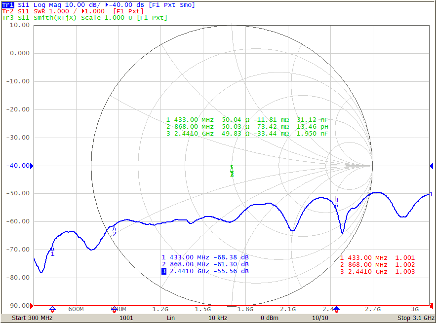 Figure 4-5 S11 Values of the Precision
Standard Calibration Kit at 868 MHz And 2440 MHz
Figure 4-5 S11 Values of the Precision
Standard Calibration Kit at 868 MHz And 2440 MHzS11 value at 868 MHz is -61.30 dB and corresponding SWR value is 1:1.002. At 2.441 GHz SWR value is 1:1.003. Meaning, after the calibration users can measure antenna SWR levels starting from 1:1.002 or 1:1.003, but not below these two levels at corresponding frequencies.
There are two methods of VNA calibration for taking the antenna measurements:
- Using the standard calibration kit, short pigtail (or cable) and port extension option.
- Using on-board calibration with open, short and matched 50 Ohm loads (SOL calibration).
The standard calibration kits are expensive, so the method of on-board calibration is more popular, but less precise.
Performing on-board calibration for in-device antenna matching brings users compromises as it’s impossible to make a precision open, short and matched loads due to parasitic elements. Users decide what is the compromise between a time being spent on board and equipment preparation for the calibration and final measured and matched results.
Below are three examples of measured 50 Ohm loads:
- Single 0402 size resistor 49.9 Ohm 0.1% (A)
- Two 0402 size resistors 100 Ohm 1% in shunt placed on top of each other (B)
- Two 0402 size resistors 100 Ohm 1% in shunt T-placement configuration (C)
The first example is shown for a single 49.9 Ohm 0.1% resistor (Figure 4-6). Measured S11, SWR and impedance are shown on Figure 4-7.
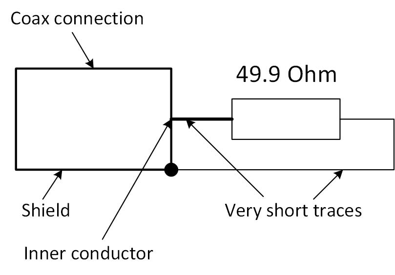 Figure 4-6 Single 49.9 Ohm Resistor
Connection
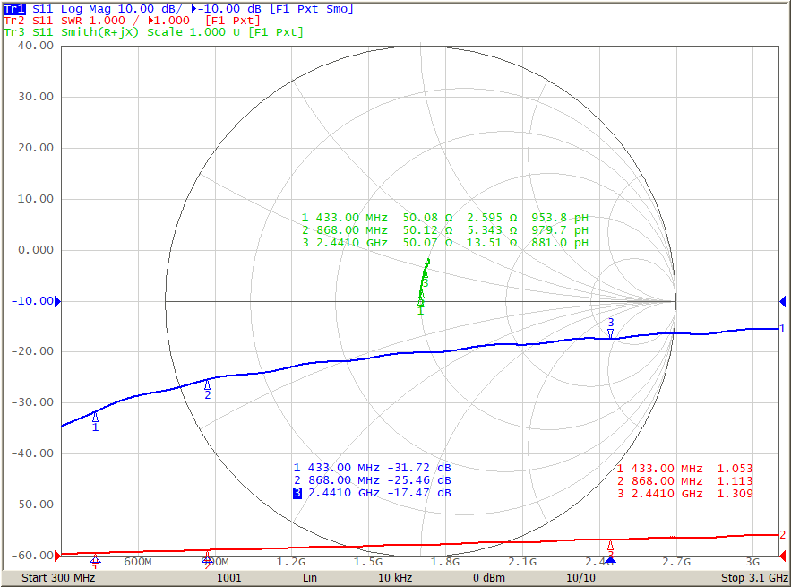 Figure 4-7 Measured Single 49.9 Ohm SMD
Resistor
Figure 4-7 Measured Single 49.9 Ohm SMD
ResistorAt 2.441 GHz the level of S11 is -17.36 dB. This means, the corresponding SWR value is 1:1.314.If VNA was calibrated with this matched load, users were unable to measure SWR below 1.314 level.
It happens due to a fact, the parasitic inductance in series with the active resistance increases with the frequency and adds about 13.51 Ohm at 2.441 GHz (Marker 3, Figure 4-7) making the total load’s (resistor’s) impedance (Z) = 51.86 Ohm. That is why users see SWR of 1:1.314.
Connecting two 100 Ohm 1% resistors in shunt and placing them on top of each other (Figure 4-8) decreases parasitic series inductance almost in double (Figure 4-9) down to 7.51 Ohm and 489 pH.
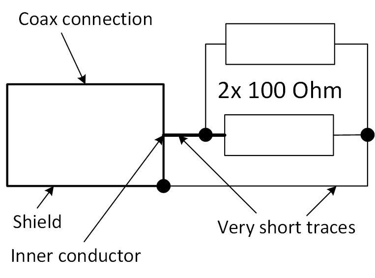 Figure 4-8 Two 100 Ohm Resistors in Shunt
Placed on Top of Each Other
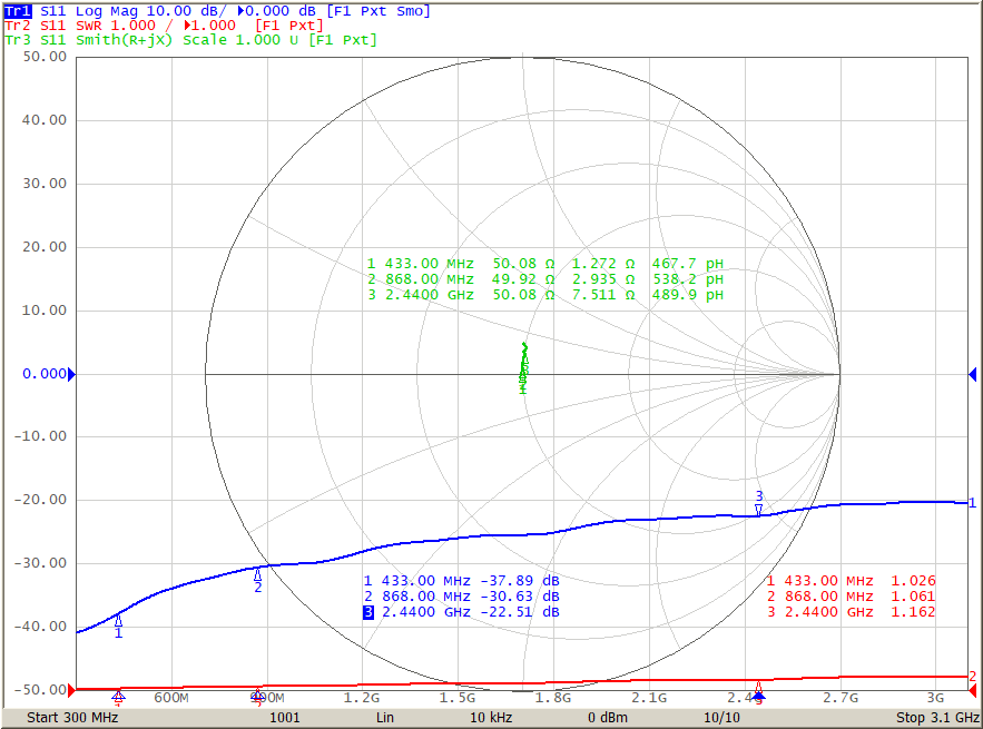 Figure 4-9 Measured Two 100 Ohm Resistors
in Shunt Placed on Top of Each Other
Figure 4-9 Measured Two 100 Ohm Resistors
in Shunt Placed on Top of Each OtherMeasured S11 values are shown on Figure 4-9. S11 improved down to - 22.51 dB with the corresponding SWR value of 1:1.162 at 2.441 GHz frequency.
Resistors T-placement configuration (Figure 4-10) gives highest accuracy, but requires a very short and solid ground plane with proper termination. Measured impedances and S11 levels are shown on Figure 4-11.
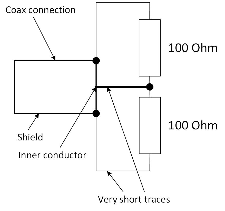 Figure 4-10 Resistors T-Placement
In reality such configuration is possible on PCB, but requires high quality cable connection to the board and short lines (matched traces) with a good, short and solid ground plane as a current return path. This means, for low power transceivers and real traces with their configuration on PCB it’s almost impossible to implement.
Users can place the resistors on PCB in such configuration, but it will not bring any valuable improvements in comparison to two 100 Ohm resistors in a shunt scheme placed on top of each other.
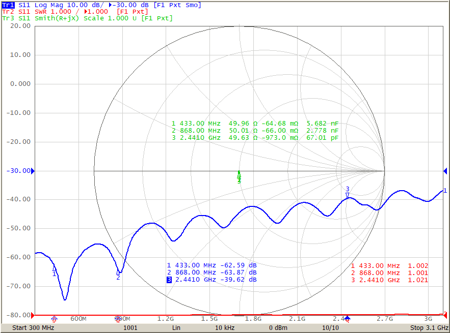 Figure 4-11 Measured Two 100 Ohm Resistors
in Shunt in T-Placement
Figure 4-11 Measured Two 100 Ohm Resistors
in Shunt in T-PlacementCorresponding SWR level to S11 value of - 39.62 dB is 1:1.021 at 2440 MHz (marker 3). It’s a decently good level for the custom 50 Ohm load.
Precise and matched to 50 Ohm load allows users to measure the lowest SWR value. Less precise load can offset SWR level and make possible VNA to measure SWR value higher than it is.
Figure 4-12 and Figure 4-13 show SWR and S11 parameters for the 868 MHz antenna measured at the same operation environment conditions, but VNA calibrations were made using loads (A) and (C) from the examples above.
Users can see, less precise load gives the highest measured SWR value of the antenna (1:1.636 versus 1:1.457).
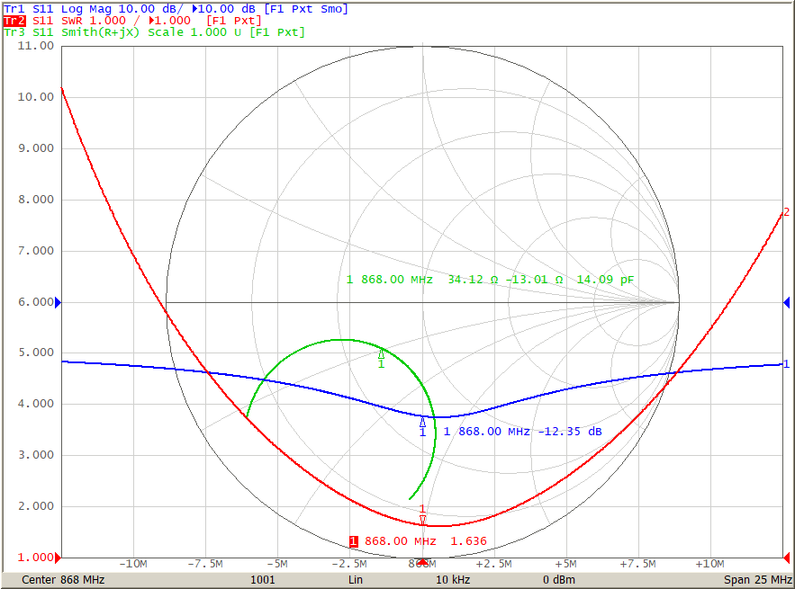 Figure 4-12 Measured Results After VNA
Calibration Using Load (A)
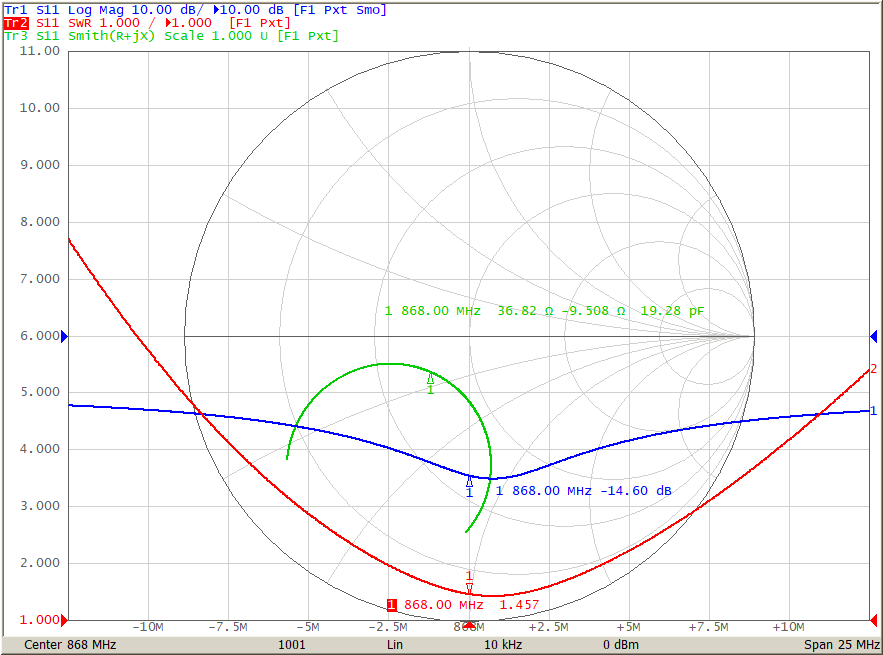 Figure 4-13 Measured Results After VNA
Calibration Using Load (C)
Figure 4-13 Measured Results After VNA
Calibration Using Load (C)Interesting to understand, that calibration load’s quality can affect a precise load measurement. Because VNA is thinking, that he was calibrated with a reference load and compares this reference to other loads. This means, the most precision load can be measured as having worst parameters. And this how the VNA operates. If users want to get most accurate measurements, VNA should be calibrated with the most precision load.
An example of such VNA operation is shown on Figure 4-14. VNA was calibrated by the load from the above example (A). The loads (B) and (C) were measured for S11. Users can see, the most accurate load (C) measured as having worst S11 parameter.
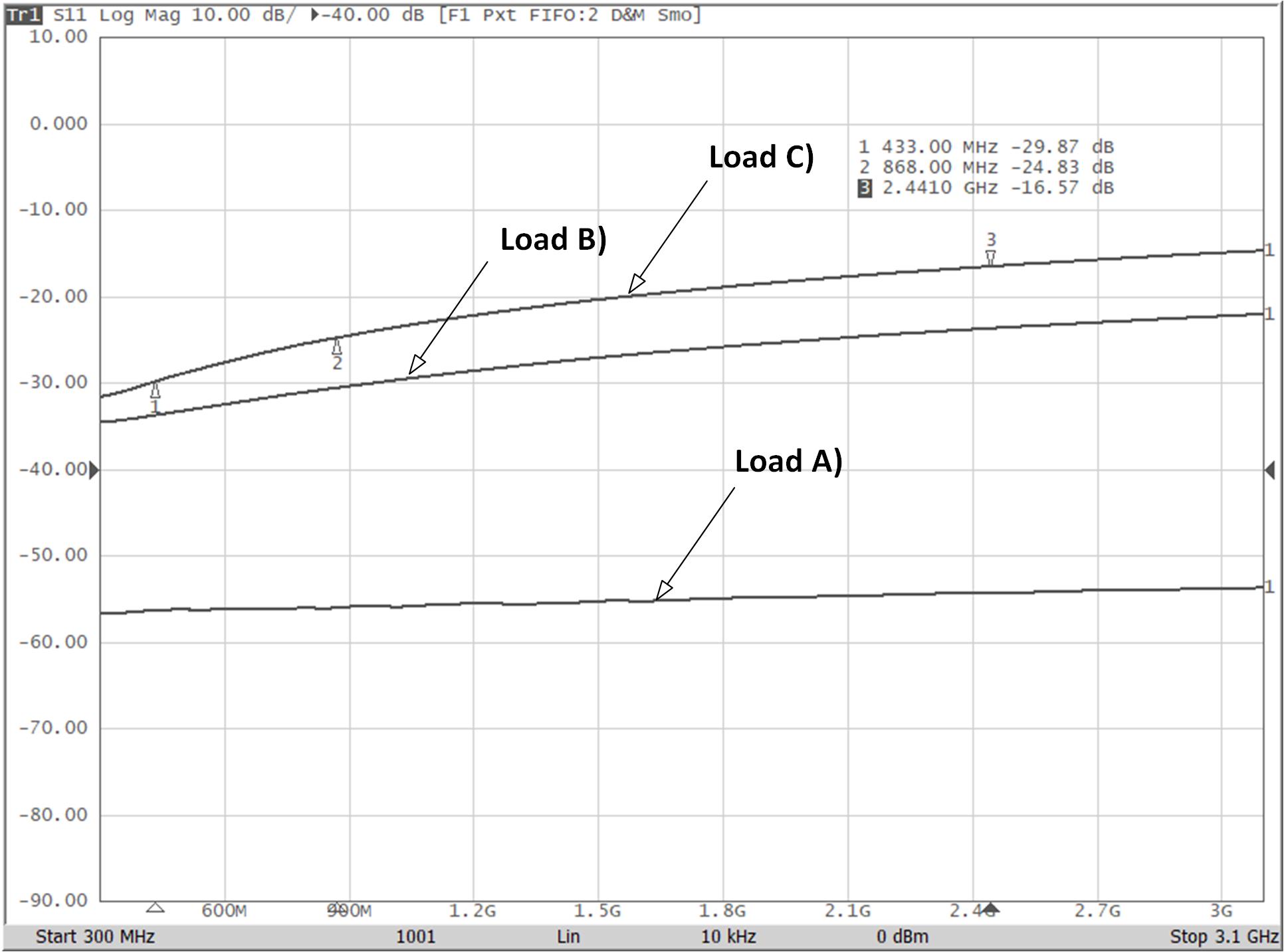 Figure 4-14 Loads S11 Parameter
Measurements
Figure 4-14 Loads S11 Parameter
MeasurementsMaking the custom calibration loads can be sufficient for frequencies up to 6 GHz. But many nuances have to be considered. Main question is how and to what the custom calibration loads can be compared. Precision calibration kit can help to answer this question.
If users don’t have an access to the precision calibration kit, the on-board calibration can be sufficient in many cases for proper antenna matching, but users need to pay attention to cable and soldering quality. In addition, proper layout techniques can help to decrease the parasitics.
4.3 VNA Calibration Procedure
Calibration method described below can’t be high precise as it’s impossible to make a precision short, open and matched loads on the board, especially for frequencies above 2 GHz due to parasitic elements (short load will always have an inductance and open load a fringing capacitance), but reasonably sufficient for antenna in-device measurement and matching.
An example of typical Pi-matching network (not in scale) and DC blocking capacitor on PCB are shown on Figure 4-15.
 Figure 4-15 Typical Matching Network
Matching components should be removed (if not already) from the board and matching network isolated from a transceiver (for example, removed DC blocking capacitor). An example with connected semi-rigid cable and SOL calibration point is shown on Figure 4-16.
 Figure 4-16 Example of Semi-Rigid Coaxial Cable Connection to Matching Network
- For
calibration “Open” load - solder the shield to main PCB ground plane close to
antenna’s feed point and leave an inner conductor unconnected (Figure 4-17).
 Figure 4-17 VNA Calibration for
Open Load
 - For calibration “Short” load -
solder the inner conductor to the shield. In this example SMD jumper of 0 Ohm
was used (Figure 4-18).
 Figure 4-18 VNA Calibration for
Short Load
 - For calibration matched 50 Ohm
“Load” – two shunt SMD resistors of 100 Ohm each (or one of 49.9 Ohm or 50 Ohm)
can be used. The resistors should be soldered to the inner conductor and shield
(Figure 4-19).
 Figure 4-19 VNA Calibration for
Matched 50-Ohm Load
Depending on what VNA model users use, an option for delay can have different menu name (for example, port extension). Port extension allows users to move electrically a measurement reference plane after the calibration.
Figure 4-20 shows uncompensated delay after the calibration with short load connected at 868 MHz frequency. So, the VNA is showing connected short load as not the short load. If the compensation will not be done, it can compromise measured impedance value of the antenna, so the final matching of the antenna will be incorrect and far in comparison with a real antenna’s behavior.
 Figure 4-20 Uncompensated Delay with
Short-Load Connected
Figure 4-20 Uncompensated Delay with
Short-Load ConnectedAfter the compensation, the marker should indicate the Short load. Compensated delay of 32.82 ps is shown on Figure 4-21.
 Figure 4-21 Compensated Delay with
Short-Load Connected
Figure 4-21 Compensated Delay with
Short-Load ConnectedCompensation (port extension) can be done with open load as well. The short load just better as gives higher level of reflections to VNA port. In reality, short and open loads have slightly different delays even for the precision calibration kits.
It is good practice to measure losses (skin effect losses) and compensate them if VNA supports this feature.
5 868-MHz PCB Helix Antenna Measurement and Matching
This chapter describes the PCB helix antenna impedance measurement and matching procedure. A detailed description of this type of antenna with 3D radiation diagrams are in the Design Note DN038.
For antenna impedance measurement users can install SMD jumper (Figure 5-1). This will connect the cable to the antenna including matching network traces.
 Figure 5-1 Installed SMD Jumper
Figure 5-2 shows the measured results of unmatched helix antenna. The impedance at 868 MHz is 15.0 – j13.8 Ohm (marker 1). SWR at this frequency is 3.60:1. The antenna must be matched to get better SWR value. At 3.60:1, the device will lose about 30% power.
 Figure 5-2 Measured Impedance of
Unmatched 868-MHz Helix Antenna
Figure 5-2 Measured Impedance of
Unmatched 868-MHz Helix AntennaUsing Figure 4-4, users can determine that to move marker 1 to the center of the chart, 4-4C or 4-4D can be chosen.
Components values can be known by using an online Smith chart calculator. There are many types on the Internet with different functions and options. Users can choose any or multiple to compare results. Links to a few of the online Smith calculators are shown below.
Links to online Smith calculators:
- http://www.iowahills.com/Index.html
- https://www.optenni.com/
- https://www.awr.com
- http://cgi.www.telestrian.co.uk/
- https://www.will-kelsey.com/smith_chart/
- https://www.fritz.dellsperger.net/smith.html
Calculated ideal values (Figure 5-3).
- network 4-4C: 4.7 nH and 5.3 pF
- network type 4-4D: 8.8 pF and 6.2 nH
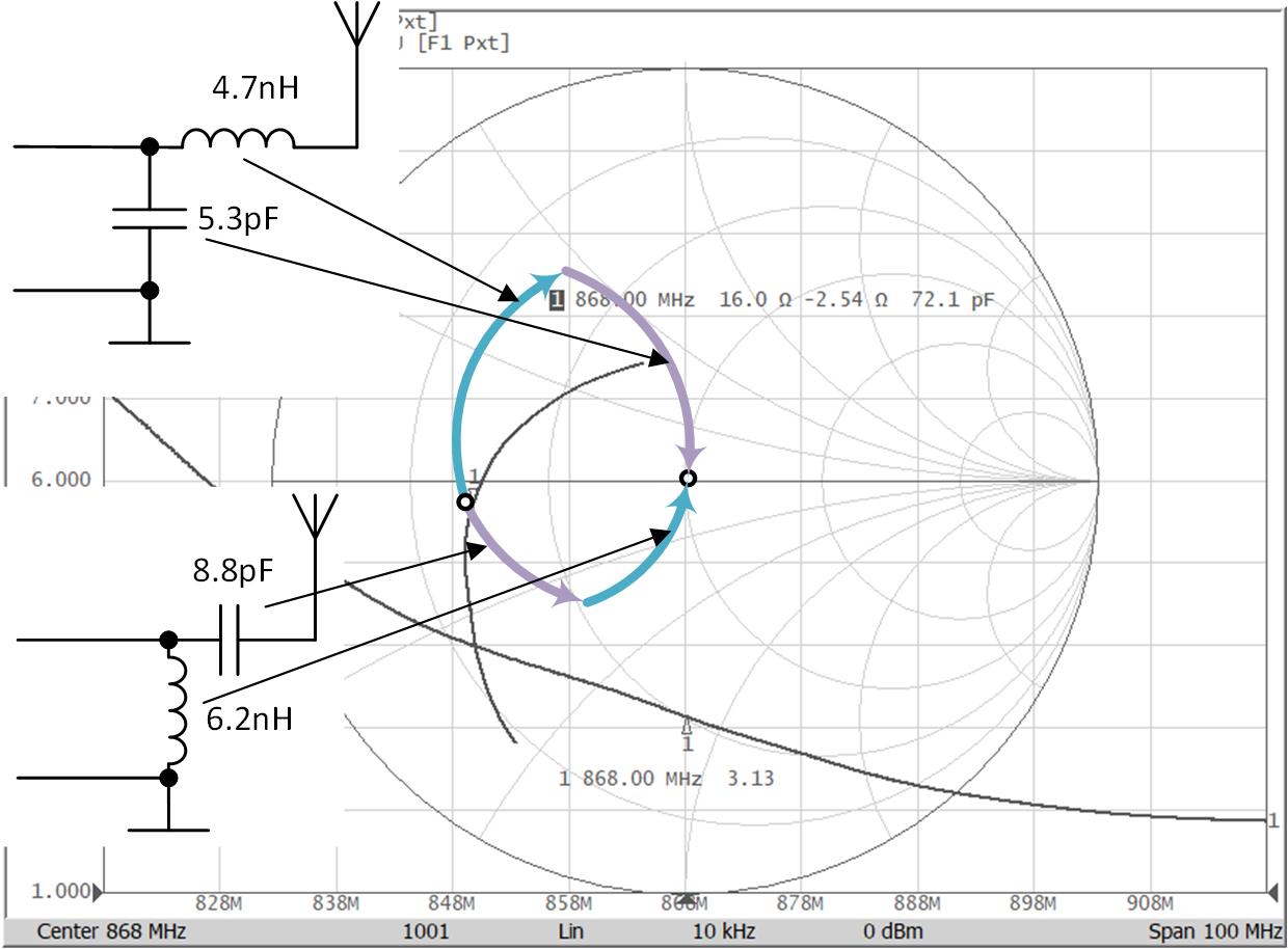 Figure 5-3 Calculated Ideal Components
Values
Figure 5-3 Calculated Ideal Components
ValuesTo better understand what type of the network is more useful, users can change component values to see how they will move the impedance on the chart (if the calculator supports this feature). Sometimes, the network can be sensitive to components values, so users may see that tolerances can move the impedance far and detune the antenna. Also note, most of the calculators use ideal components values, so a final value’s tuning should be made.
Figure 5-3 shows passive component arcs with different colors. Colors represent what way the impedance transforms. Ideally, a value of 4.7 nH should move marker 1 to upper side of Volpert-Smith chart. In reality it does, but due to component tolerance and parasitic (including PCB) the final point will be different. You can connect VNA and look where the marker is and adjust the value if needed.
If users install two matching components simultaneously on board users will spend more time figuring out which of them and what value should change to get desired impedance and SWR level. Figure 5-4 shows what way marker 1 moved if the only 5.1 nH inductor installed (for network 4-4C).
 Figure 5-4 Measured Impedance for Network
4-4C (with 5.1 nH, No Capacitor Installed)
Figure 5-4 Measured Impedance for Network
4-4C (with 5.1 nH, No Capacitor Installed)Leave 5.1 nH value and add a shunt capacitor of 5.1 pF (0.3 pF less than ideal calculated value). Measured impedance is shown on (Figure 5-5).
 Figure 5-5 Measured Impedance for Network
4-4C (with 5.1 pF and 5.1 nH)
Figure 5-5 Measured Impedance for Network
4-4C (with 5.1 pF and 5.1 nH)The line crossed and the value of 5.1 pF should be decreased, but not much. Install 4.7 pF and measure the impedance (Figure 5-6).
 Figure 5-6 Measured Impedance for Network
4-4C (with 4.7 pH and 5.1 nH)
Figure 5-6 Measured Impedance for Network
4-4C (with 4.7 pH and 5.1 nH)Marker moves closer to 50 Ohm point with SWR improvement, and users can try to install 4.2 pF capacitor and measure the result (Figure 5-7).
 Figure 5-7 Measured Impedance for Network 4-4C (with 4.2 pF and 5.1 nH)
It’s just 0.5 pF capacitance changing (from 4.7 pF down to 4.2 pF), but marker moves too fast. Now users can try to move the marker a little bit left to get closer to 50 Ohm point by decreasing of inductance from 5.1 nH down to 4.7 nH (Figure 5-8).
 Figure 5-8 Measured Impedance for Network 4-4C (with 4.2 pF and 4.7 nH)
Marker is moving around 50 Ohm point due to steps of standard components values. In this particular case the network configuration 4-4C is sensitive to components values. That means in real applications with mass production and components tolerances the impedance will change a lot with corresponded SWR value. It also shown on Figure 5-3. For the network 4-4C the smaller components values move the marker faster, than network’s 4-4D higher values.
Users can also try the network 4-4D. Just not to overload the document by the figures, the same steps were made as for 4-4C above:
- Installed the capacitor of 9.1 pF in series with the antenna to check how far the marker moves.
- Installed an inductor of 6.2 nH in shunt and measured the impedance.
- Decreased capacitor value down to 8.2 pF to get closer to 50 Ohm point.
A final matched result with 8.2 pF and 6.2 nH is shown on Figure 5-9 with SWR value of 1:1.07.
 Figure 5-9 Measured Impedance and SWR for Network 4-4D (with 8.2 pF and 6.2 nH)
Both networks can be tuned further to get better match. Users must decide what values of impedance and SWR are optimum.
6 2.4-GHz PCB Compact Antenna Measurement and Matching
Antenna matching described in this chapter is showing an example of cased 2.4-GHz PCB compact (15 mm by 6 mm) antenna (Figure 6-1). This antenna is popular for portable devices with space constrained boards as it has small geometrical sizes. Detailed antenna description can be found on document AN043.
 Figure 6-1 Compact 2.4 GHz PCB
Antenna
Figure 6-1 Compact 2.4 GHz PCB
AntennaPortable devices are usually made for in-hand operation. Plastic case and human’s body can detune the antenna. In such case, a final matching should be done including the case and human’s body, representing a real device’s operation condition. Figure 6-2 is showing measured SWR values in free space, in a plastic case and in the plastic case with in-hand placement.
 Figure 6-2 Measured SWR Levels
Users can see the SWR value changes from 1:1.70 (in free space) up to 1:3.68 when antenna is cased and placed in hand.
For given impedance of 19.2 + j30.4 Ohm (at 2.4410 GHz) Smith calculator shows ideal components values for matching network 4-4A of 1.9 pF plus 3.5 nH.
It’s important to remember, the calculator gives the ideal values. But for matching job, especially with human’s body affecting the antenna, the final matching circuit can be different.
For matching job, the only capacitor of 1.8 pF installed. Measured impedance with plastic and in-hand placement shown on Figure 6-3.
 Figure 6-3 Measured Impedance with 1.8 pF
Capacitor Installed
Figure 6-3 Measured Impedance with 1.8 pF
Capacitor InstalledLooking at measured marker 1 and Smith calculator’s chart gives an idea that parasitic capacitance is about 0.5 pF. This means the value can be adjust down to about 1.2 pF. Figure 6-4 shows measured impedance with 1.5 pF installed.
 Figure 6-4 Measured Impedance with 1.5 pF
Capacitor Installed
Figure 6-4 Measured Impedance with 1.5 pF
Capacitor InstalledFor this matching job even doesn’t necessary to install the inductor and it can be replaced by SMD jumper (Figure 6-5) as SWR value is 1:1.05.
 Figure 6-5 Board with Installed Final
Matching Components
Figure 6-5 Board with Installed Final
Matching Components7 2.4-GHz PCB Inverted-F Antenna Measurement and Matching
A PCB inverted-F antenna is popular for Bluetooth®, Bluetooth® Low Energy, and ZigBee™ devices. It also can be used for Wi-Fi™ applications. Users can find the antenna's detailed description in the Application report DN007
The board was prepared for the tests and VNA calibration was done including matching network traces (refer to the Section 4.2).
 Figure 7-1 PCB Inverted-F Antenna
The impedance and SWR of unmatched antenna are shown in Figure 7-2. Markers are showing low, mid, and high operation frequencies for Bluetooth Low Energy and ZigBee applications. At 2.4410 GHz, the impedance is 29.5 + j11.5 Ohm and SWR value is 1.83:1.
 Figure 7-2 Measured Impedance of
Unmatched PCB Inverted-F Antenna at 2.4410 GHz
Figure 7-2 Measured Impedance of
Unmatched PCB Inverted-F Antenna at 2.4410 GHzFigure 4-4 shows that the network 4-4C and 4-4D can move the impedance to the center of the chart.
Online Smith chart calculators for the frequency at 2441 MHz and given impedance of 29.5 + j11.5 Ohm for network 4-4C gave values of 0.9 nH plus 1.1 pF. For small value capacitances (≤ 2 pF) usually recommended to pull back the ground plane a little on the top layer (not to affect the final capacitance and to use tight tolerances).
The network 4-4D with components values of 1.8 pF plus 3.9 nH was used. For matching job next steps were made:
- The only capacitor of 1.8 pF was installed for checking how far the marker moves
(Figure 7-3).
 Figure 7-3 Measured Impedance
with only 1.8 pF Capacitor Installed
 - Installed inductor of 3.9 nH (1.8 pF and 3.9 nH)
- Adjusted inductor’s value to 4.3 nH (1.8 pF and 4.3 nH)
- Adjusted capacitor’s value to 2.0 pF (2.0 pF and 4.3 nH)
Figure 7-4 shows a final matched impedance with corresponded SWR and S11 levels. SWR value improved from 1:1.83 down to 1:1.08.
 Figure 7-4 Measured Impedance, SWR, and
S11 for Network 4-4D (with 2.0 pF and 4.3 nH)
 Figure 7-5 Board with Final Matching
Components Installed
Figure 7-5 Board with Final Matching
Components Installed8 Fast in-circuit or in-device Antenna Verification
There is a fast method for in-circuit or in-device embedded antenna verification/checking. Users can verify or check if the antenna has desired resonant frequency, matching or bandwidth without any soldering.
For this task a reflectometer (or VNA), flexible high-quality cable, handmade pigtail and standard calibration kit need to be used. An example below made by using the CABAN R60 reflectometer (cable and antenna analyzer) made by PLANAR LLC (or R60 model by Copper Mountain Technologies) and R VNA Software application.
 Figure 8-1 Vector Reflectometer CABAN
R60
Figure 8-1 Vector Reflectometer CABAN
R60Small in size and portable reflectometer allows users to test the antenna outside of the lab or in fields. Such cases can be, for example, a smoke detector mounted on a wall, device on a human's body or low power wireless transceiver mounted near metal water pipes (for water/gas meters).
High quality cables are important as measured data will depend on the cable's movement. High quality cables have low instability on movement, so the data will not fluctuate much.
The calibration kit is 03K30R-MSOTS3 by Rosenberger used for calibration.
The pigtail can be made by using a short semi-rigid cable with SMA connector and ground (pogo) pin Figure 8-2. Ground pogo pin can help to get a robust connection and compensate connector’s length mismatch.
 Figure 8-2 Handmade Pigtail
A picture of the setup is shown on Figure 8-3.
 Figure 8-3 Test Setup
Before taking the antenna's measurement, the CABAN R60 vector reflectometer should be calibrated with the standard calibration kit for open, short and matched loads including cable and adapters.
After the calibration users can connect their handmade pigtail to the cable and compensate for phase delay (to move a reference plane) through the port extension option for open load, as the pigtail has opened connectors Figure 8-4.
 Figure 8-4 Calibration Method Using Port Extension Option
Uncompensated phase delay due to connected pigtail for open load is shown on Figure 8-5.
 Figure 8-5 Uncompensated Phase Delay After Pigtail Connection
For the port extension option, it’s a good idea to include and compensate a skin effect loss (Include Loss) by switching on a corresponded menu option Figure 8-6.
 Figure 8-6 Port Extension Option
Compensated delay after the enabled port extension option is shown on Figure 8-7. Phase compensation allows the impedance to be measured correctly.
 Figure 8-7 Compensated Phase Delay For The Connected Pigtail
Below is an example of measured SWR of an 868-MHz antenna for the same operation conditions made by a connected cable (gray curve) and a connected pigtail (black curve). As users can see there is not much difference in measurements Figure 8-8.
A hand in the nearest zone with the antenna detunes her a little, but anyway allows to check the antenna's resonant frequency and SWR value without any soldering.
 Figure 8-8 Measured Resonant Frequencies and SWR Levels
9 Conclusion
The examples above use 868-MHz and 2.4-GHz band antennas, but similar measurement and matching techniques can be implemented for any frequency range and any type of antenna.
Consider future antenna parameters at the designing phase. If users want to use your own specific antenna, like helical, rod, or PCB, or antenna from reference design or evaluation board, the antenna's impedance should be matched or tuned. Users cannot predict what the unmatched impedance value will be as it depends on many factors (common ground plane, casing, objects around, and so on). Without VNA at the lab it is hard to understand what the parameters of your antenna are. But at least they can be measured to minimize negative effects. So, it is better to measure and match the impedance on a real board in real conditions before a design is fixed, otherwise, there is almost nothing users can do to get better range.
For PCB design users can refer to a document: CC13xx/CC26xx Hardware Configuration and PCB Design Considerations (Rev. F). For crystal selection refer to a document: Crystal Oscillator and Crystal Selection for the CC26xx and CC13xx Wireless MCUs (Rev. I).
Components 0201 of size are preferable, especially for matching, as they have tight tolerances and small value step, for example, capacitors kit muRata p/n: GJM03-KIT-TTOL-DE or Wurth Elektronik capacitors and inductors kits 744 765 and 885 390 can be used.
Use Pi-network layout on a board at least for prototypes. It will help to use most of network configurations for antenna matching job.
IMPORTANT NOTICE AND DISCLAIMER
| TI PROVIDES TECHNICAL AND RELIABILITY DATA (INCLUDING DATASHEETS), DESIGN RESOURCES (INCLUDING REFERENCE DESIGNS), APPLICATION OR OTHER DESIGN ADVICE, WEB TOOLS, SAFETY INFORMATION, AND OTHER RESOURCES “AS IS” AND WITH ALL FAULTS, AND DISCLAIMS ALL WARRANTIES, EXPRESS AND IMPLIED, INCLUDING WITHOUT LIMITATION ANY IMPLIED WARRANTIES OF MERCHANTABILITY, FITNESS FOR A PARTICULAR PURPOSE OR NON-INFRINGEMENT OF THIRD PARTY INTELLECTUAL PROPERTY RIGHTS. |
| These resources are intended for skilled developers designing with TI products. You are solely responsible for (1) selecting the appropriate TI products for your application, (2) designing, validating and testing your application, and (3) ensuring your application meets applicable standards, and any other safety, security, or other requirements. These resources are subject to change without notice. TI grants you permission to use these resources only for development of an application that uses the TI products described in the resource. Other reproduction and display of these resources is prohibited. No license is granted to any other TI intellectual property right or to any third party intellectual property right. TI disclaims responsibility for, and you will fully indemnify TI and its representatives against, any claims, damages, costs, losses, and liabilities arising out of your use of these resources. |
| TI’s products are provided subject to TI’s Terms of Sale (www.ti.com/legal/termsofsale.html) or other applicable terms available either on ti.com or provided in conjunction with such TI products. TI’s provision of these resources does not expand or otherwise alter TI’s applicable warranties or warranty disclaimers for TI products. |
| Mailing Address: Texas Instruments, Post Office Box 655303, Dallas, Texas 75265
Copyright © 2021, Texas Instruments Incorporated |