CSD16340Q3 25-V N-Channel NexFET Power MOSFET
1 Features
- Optimized for 5 V Gate Drive
- Resistance Rated at VGS =2.5 V
- Ultra-Low Qg and Qgd
- Low Thermal Resistance
- Avalanche Rated
- Pb Free Terminal Plating
- RoHS Compliant
- Halogen Free
- SON 3.3-mm × 3.3-mm Plastic Package
2 Applications
- Point of Load Synchronous Buck Converter for Applications in Networking, Telecom, and Computing Systems
- Optimized for Control or Synchronous FET Applications
3 Description
This 25 V, 3.8 mΩ, 3.3 × 3.3 mm SON NexFET™ power MOSFET is designed to minimize losses in power conversion and optimized for 5 V gate drive applications.
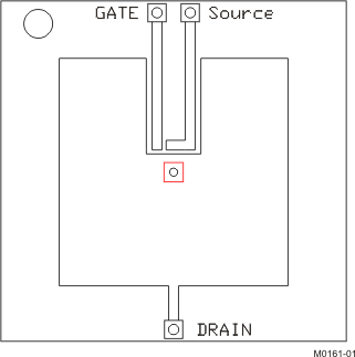
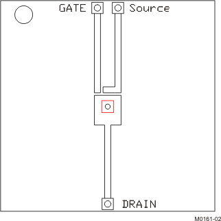
Top View

Product Summary
Ordering Information(1)
| Device | Media | Qty | Package | Ship |
|---|---|---|---|---|
| CSD16340Q3 | 13-Inch Reel | 2500 | SON 3.3 x 3.3 mm Plastic Package | Tape and Reel |
| CSD16340Q3T | 7-Inch Reel | 250 |
- For all available packages, see the orderable addendum at the end of the data sheet.
Absolute Maximum Ratings
| TA = 25°C | VALUE | UNIT | |
|---|---|---|---|
| VDS | Drain-to-Source Voltage | 25 | V |
| VGS | Gate-to-Source Voltage | +10 / –8 | V |
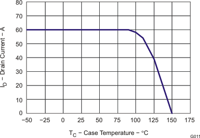
| ID | Continuous Drain Current, TC = 25°C | 60 | A |
| Continuous Drain Current(1) | 21 | A | |
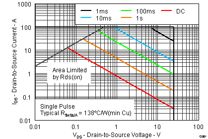
| IDM | Pulsed Drain Current, TA = 25°C(2) | 115 | A |
| PD | Power Dissipation(1) | 3 | W |
| TJ, Tstg |
Operating Junction and Storage Temperature Range |
–55 to 150 | °C |
| EAS | Avalanche Energy, single pulse ID = 40 A, L = 0.1 mH, RG = 25 Ω |
80 | mJ |
- Typical RθJA = 39°C/W on 1in2 Cu (2 oz.) on 0.060" thick FR4 PCB.
- Pulse width ≤300 μs, duty cycle ≤2%
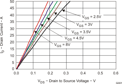
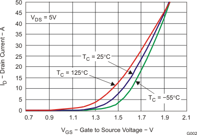
RDS(on) vs VGS |
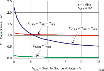
Gate Charge |
4 Revision History
Changes from D Revision (November 2011) to E Revision
Changes from C Revision (June 2011) to D Revision
- Replaced the THERMAL CHARACTERISTICS table with the new Thermal Information TableGo
- Replaced Figure 10 - Maximum Safe Operating AreaGo
Changes from B Revision (September 2010) to C Revision
- Deleted the Package Marking Information section Go
Changes from A Revision (January 2010) to B Revision
Changes from * Revision (December 2009) to A Revision
- Changed Qg in the PRODUCT SUMMARY table from: 6.8 To 6.5 nCGo
5 Specifications
5.1 Electrical Characteristics
(TA = 25°C unless otherwise stated)| PARAMETER | TEST CONDITIONS | MIN | TYP | MAX | UNIT | ||
|---|---|---|---|---|---|---|---|
| STATIC CHARACTERISTICS | |||||||
| BVDSS | Drain-to-Source Voltage | VGS = 0 V, IDS = 250 μA | 25 | V | |||
| IDSS | Drain-to-Source Leakage Current | VGS = 0 V, VDS = 20 V | 1 | μA | |||
| IGSS | Gate-to-Source Leakage Current | VDS = 0 V, VGS = +10/–8 V | 100 | nA | |||
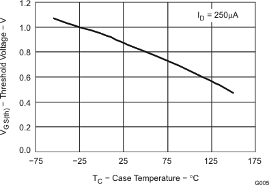
| VGS(th) | Gate-to-Source Threshold Voltage | VDS = VGS, IDS = 250 μA | 0.6 | 0.85 | 1.1 | V | |
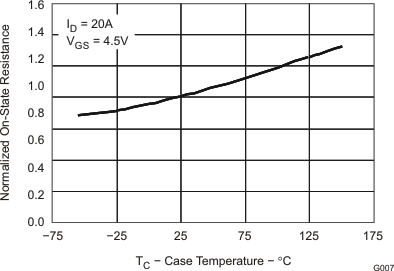
| RDS(on) | Drain-to-Source On-Resistance | VGS = 2.5 V, IDS = 20 A | 6.1 | 7.8 | mΩ | ||
| VGS = 4.5 V, IDS = 20 A | 4.3 | 5.5 | mΩ | ||||
| VGS = 8 V, IDS = 20 A | 3.8 | 4.5 | mΩ | ||||
| gƒs | Transconductance | VDS = 15 V, IDS = 20 A | 121 | S | |||
| DYNAMIC CHARACTERISTICS | |||||||
| CISS | Input Capacitance | VGS = 0 V, VDS = 12.5 V, ƒ = 1 MHz | 1050 | 1350 | pF | ||
| COSS | Output Capacitance | 730 | 950 | pF | |||
| CRSS | Reverse Transfer Capacitance | 53 | 69 | pF | |||
| Rg | Series Gate Resistance | 1.5 | 3 | Ω | |||
| Qg | Gate Charge Total (4.5 V) | VDS = 12.5 V, ID = 20 A | 6.5 | 9.2 | nC | ||
| Qgd | Gate Charge Gate-to-Drain | 1.2 | nC | ||||
| Qgs | Gate Charge Gate-to-Source | 2.1 | nC | ||||
| Qg(th) | Gate Charge at Vth | 1 | nC | ||||
| QOSS | Output Charge | VDS = 13 V, VGS = 0 V | 15 | nC | |||
| td(on) | Turn On Delay Time | VDS = 12.5 V, VGS = 4.5 V, ID = 20 A RG = 2 Ω |
4.8 | ns | |||
| tr | Rise Time | 16.1 | ns | ||||
| td(off) | Turn Off Delay Time | 13.8 | ns | ||||
| tƒ | Fall Time | 5.2 | ns | ||||
| DIODE CHARACTERISTICS | |||||||
| VSD | Diode Forward Voltage | IS = 20 A, VGS = 0 V | 0.8 | 1 | V | ||
| Qrr | Reverse Recovery Charge | VDD = 13 V, IF = 20 A, di/dt = 300 A/μs | 14.5 | nC | |||
| trr | Reverse Recovery Time | 20 | ns | ||||
5.2 Thermal Information
| THERMAL METRIC(1)(2) | CSD16340Q3 | UNITS | |
|---|---|---|---|
| Q3 (8 PINS) | |||
| θJA | Junction-to-Ambient Thermal Resistance | 42.0 | °C/W |
| θJCtop | Junction-to-Case (top) Thermal Resistance | 20.6 | |
| θJB | Junction-to-Board Thermal Resistance | 8.8 | |
| ψJT | Junction-to-Top Characterization Parameter | 0.3 | |
| ψJB | Junction-to-Board Characterization Parameter | 8.7 | |
| θJCbot | Junction-to-Case (bottom) Thermal Resistance | 0.1 | |
 |
Max RθJA = 58°C/W when mounted on 1 inch2 of 2 oz. Cu. |
 |
Max RθJA = 162°C/W when mounted on minimum pad area of 2 oz. Cu. |
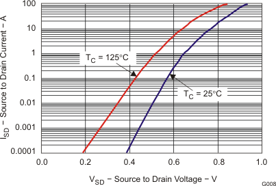
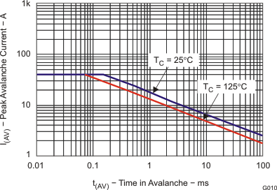
5.3 Typical MOSFET Characteristics
(TA = 25°C unless otherwise stated)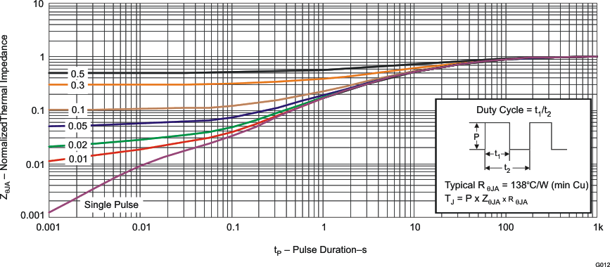
6 Device and Documentation Support
6.1 Trademarks
NexFET is a trademark of Texas Instruments.
6.2 Electrostatic Discharge Caution

These devices have limited built-in ESD protection. The leads should be shorted together or the device placed in conductive foam during storage or handling to prevent electrostatic damage to the MOS gates.
6.3 Glossary
SLYZ022 — TI Glossary.
This glossary lists and explains terms, acronyms, and definitions.