DATA SHEET
CSD17559Q5 30-V N-Channel NexFET Power MOSFET
1 Features
- Extremely Low Resistance
- Ultra-Low Qg and Qgd
- Low Thermal Resistance
- Avalanche Rated
- Pb Free Terminal Plating
- RoHS Compliant
- Halogen Free
- SON 5 mm × 6 mm Plastic Package
2 Applications
- Point of Load Synchronous Buck in Networking, Telecom, and Computing Systems
- Synchronous Rectification
- Active ORing and Hotswap Applications
3 Description
This 30 V, 0.95 mΩ, 5 × 6 mm SON NexFET™ power MOSFET is designed to minimize losses in synchronous rectification and other power conversion applications.
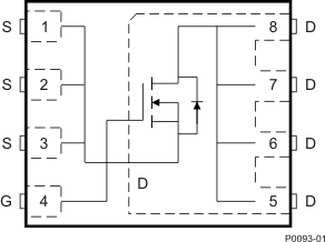
Top View
Product Summary
| TA = 25°C | TYPICAL VALUE | UNIT | ||
|---|---|---|---|---|
| VDS | Drain-to-Source Voltage | 30 | V | |
| Qg | Gate Charge Total (4.5 V) | 39 | nC | |
| Qgd | Gate Charge Gate-to-Drain | 9.3 | nC | |
| RDS(on) | Drain-to-Source On-Resistance | VGS = 4.5 V | 1.15 | mΩ |
| VGS = 10 V | 0.95 | mΩ | ||
| VGS(th) | Threshold Voltage | 1.4 | V | |
Ordering Information(1)
| Device | Qty | Media | Package | Ship |
|---|---|---|---|---|
| CSD17559Q5 | 2500 | 13-Inch Reel | SON 5 × 6 mm Plastic Package | Tape and Reel |
| CSD17559Q5T | 250 | 13-Inch Reel |
- For all available packages, see the orderable addendum at the end of the data sheet.
Absolute Maximum Ratings
| TA = 25°C | VALUE | UNIT | |
|---|---|---|---|
| VDS | Drain-to-Source Voltage | 30 | V |
| VGS | Gate-to-Source Voltage | ±20 | V |
| ID | Continuous Drain Current (Package limited) | 100 | A |
| Continuous Drain Current (Silicon limited), TC = 25°C | 257 | ||
| Continuous Drain Current(1) | 40 | A | |
| IDM | Pulsed Drain Current(2) | 400 | A |
| PD | Power Dissipation(1) | 3.2 | W |
| Power Dissipation, TC = 25°C | 96 | ||
| TJ, Tstg |
Operating Junction and Storage Temperature Range |
–55 to 150 | °C |
| EAS | Avalanche Energy, single pulse ID = 104 A, L = 0.1m H, RG = 25 Ω |
541 | mJ |
RDS(on) vs VGS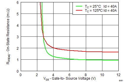 |
Gate Charge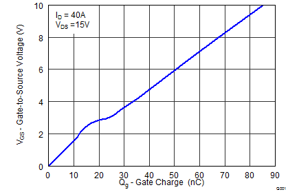 |
4 Revision History
Changes from * Revision (Novermber 2012) to A Revision
5 Specifications
5.1 Electrical Characteristics
(TA = 25°C unless otherwise stated)| PARAMETER | TEST CONDITIONS | MIN | TYP | MAX | UNIT | ||
|---|---|---|---|---|---|---|---|
| STATIC CHARACTERISTICS | |||||||
| BVDSS | Drain-to-Source Voltage | VGS = 0 V, IDS = 250 μA | 30 | V | |||
| IDSS | Drain-to-Source Leakage Current | VGS = 0 V, VDS = 24 V | 1 | μA | |||
| IGSS | Gate-to-Source Leakage Current | VDS = 0 V, VGS = 20 V | 100 | nA | |||
| VGS(th) | Gate-to-Source Threshold Voltage | VDS = VGS, IDS = 250 μA | 1.2 | 1.4 | 1.7 | V | |
| RDS(on) | Drain-to-Source On-Resistance | VGS = 4.5 V, IDS = 40 A | 1.15 | 1.5 | mΩ | ||
| VGS = 10 V, IDS = 40 A | 0.95 | 1.15 | mΩ | ||||
| gƒs | Transconductance | VDS = 15 V, IDS = 40 A | 235 | S | |||
| DYNAMIC CHARACTERISTICS | |||||||
| Ciss | Input Capacitance | VGS = 0 V, VDS = 15 V, ƒ = 1 MHz |
7070 | 9200 | pF | ||
| Coss | Output Capacitance | 1780 | 2314 | pF | |||
| Crss | Reverse Transfer Capacitance | 87 | 113 | pF | |||
| RG | Series Gate Resistance | 1.2 | 2.4 | Ω | |||
| Qg | Gate Charge Total (4.5 V) | VDS = 15 V, IDS = 40 A | 39 | 51 | nC | ||
| Qgd | Gate Charge Gate-to-Drain | 9.3 | nC | ||||
| Qgs | Gate Charge Gate-to-Source | 14.4 | nC | ||||
| Qg(th) | Gate Charge at Vth | 8.3 | nC | ||||
| Qoss | Output Charge | VDS = 15 V, VGS = 0 V | 50 | nC | |||
| td(on) | Turn On Delay Time | VDS = 15 V, VGS = 4.5 V, IDS = 40 A, RG = 2 Ω |
20 | ns | |||
| tr | Rise Time | 41 | ns | ||||
| td(off) | Turn Off Delay Time | 32 | ns | ||||
| tƒ | Fall Time | 14 | ns | ||||
| DIODE CHARACTERISTICS | |||||||
| VSD | Diode Forward Voltage | ISD = 40 A, VGS = 0 V | 0.8 | 1 | V | ||
| Qrr | Reverse Recovery Charge | VDD= 15 V, IF = 40 A, di/dt = 300 A/μs | 80 | nC | |||
| trr | Reverse Recovery Time | 37 | ns | ||||
5.2 Thermal Information
(TA = 25°C unless otherwise stated)| THERMAL METRIC | MIN | TYP | MAX | UNIT | |
|---|---|---|---|---|---|
| RθJC | Junction-to-Case Thermal Resistance(1) | 1.2 | °C/W | ||
| RθJA | Junction-to-Ambient Thermal Resistance(1)(2) | 50 | |||
(1) RθJC is determined with the device mounted on a 1 inch2 (6.45 cm2), 2 oz. (0.071 mm thick) Cu pad on a 1.5 inches × 1.5 inches
(3.81 cm × 3.81 cm), 0.06 inch (1.52 mm) thick FR4 PCB. RθJC is specified by design, whereas RθJA is determined by the user’s board design.
(3.81 cm × 3.81 cm), 0.06 inch (1.52 mm) thick FR4 PCB. RθJC is specified by design, whereas RθJA is determined by the user’s board design.
(2) Device mounted on FR4 material with 1 inch2 (6.45 cm2), 2 oz. (0.071 mm thick) Cu.
 |
Max RθJA = 50°C/W when mounted on 1 inch2 (6.45 cm2) of 2-oz. (0.071-mm thick) Cu. |
 |
Max RθJA = 125°C/W when mounted on a minimum pad area of 2-oz. (0.071-mm thick) Cu. |
5.3 Typical MOSFET Characteristics
(TA = 25°C unless otherwise stated)


