-
CSD17578Q5A 30 V N-Channel NexFET Power MOSFETs
Package Options
Refer to the PDF data sheet for device specific package drawings
Mechanical Data (Package|Pins)
- DQJ|8
Thermal pad, mechanical data (Package|Pins)
Orderable Information
CSD17578Q5A 30 V N-Channel NexFET Power MOSFETs
1 Features
- Low Qg and Qgd
- Low RDS(on)
- Low Thermal Resistance
- Avalanche Rated
- Pb-Free Terminal Plating
- RoHS Compliant
- Halogen Free
- SON 5 mm × 6 mm Plastic Package
2 Applications
- Point-of-Load Synchronous Buck Converter for Applications in Networking, Telecom, and Computing Systems
- Optimized for Control FET Applications
3 Description
This 30 V, 5.9 mΩ, SON 5 mm x 6 mm NexFET™ power MOSFET is designed to minimize losses in power conversion applications.

Product Summary
| TA = 25°C | TYPICAL VALUE | UNIT | ||
|---|---|---|---|---|
| VDS | Drain-to-Source Voltage | 30 | V | |
| Qg | Gate Charge Total (4.5 V) | 7.9 | nC | |
| Qgd | Gate Charge Gate-to-Drain | 2.0 | nC | |
| RDS(on) | Drain-to-Source On-Resistance | VGS = 4.5 V | 7.9 | mΩ |
| VGS = 10 V | 5.9 | mΩ | ||
| VGS(th) | Threshold Voltage | 1.5 | V | |
Ordering Information(1)
| Device | Media | Qty | Package | Ship |
|---|---|---|---|---|
| CSD17578Q5A | 13-Inch Reel | 2500 | SON 5 x 6 mm Plastic Package |
Tape and Reel |
| CSD17578Q5AT | 7-Inch Reel | 250 |
- For all available packages, see the orderable addendum at the end of the data sheet.
Absolute Maximum Ratings
| TA = 25°C | VALUE | UNIT | |
|---|---|---|---|
| VDS | Drain-to-Source Voltage | 30 | V |
| VGS | Gate-to-Source Voltage | ±20 | V |
| ID | Continuous Drain Current (Package limited) | 25 | A |
| Continuous Drain Current (Silicon limited), TC = 25°C | 59 | ||
| Continuous Drain Current(1) | 16 | ||
| IDM | Pulsed Drain Current(2) | 132 | A |
| PD | Power Dissipation(1) | 3.1 | W |
| Power Dissipation, TC = 25°C | 42 | ||
| TJ, Tstg |
Operating Junction and Storage Temperature Range |
–55 to 150 | °C |
| EAS | Avalanche Energy, single pulse ID = 22 A, L = 0.1 mH |
23 | mJ |
- Typical RθJA = 40°C/W on a 1 inch2, 2 oz. Cu pad on a 0.06 inch thick FR4 PCB.
- Max RθJC = 3.8°C/W, pulse duration ≤100 μs, duty cycle ≤1%
RDS(on) vs VGS |
Gate Charge |
4 Revision History
| DATE | REVISION | NOTES |
|---|---|---|
| March 2015 | * | Initial release. |
5 Specifications
5.1 Electrical Characteristics
(TA = 25°C unless otherwise stated)| PARAMETER | TEST CONDITIONS | MIN | TYP | MAX | UNIT | ||
|---|---|---|---|---|---|---|---|
| STATIC CHARACTERISTICS | |||||||
| BVDSS | Drain-to-Source Voltage | VGS = 0 V, ID = 250 μA | 30 | V | |||
| IDSS | Drain-to-Source Leakage Current | VGS = 0 V, VDS = 24 V | 1 | μA | |||
| IGSS | Gate-to-Source Leakage Current | VDS = 0 V, VGS = 20 V | 100 | nA | |||
| VGS(th) | Gate-to-Source Threshold Voltage | VDS = VGS, ID = 250 μA | 1.1 | 1.5 | 1.9 | V | |
| RDS(on) | Drain-to-Source On-Resistance | VGS = 4.5 V, ID = 10 A | 7.9 | 9.3 | mΩ | ||
| VGS = 10 V, ID = 10 A | 5.9 | 6.9 | mΩ | ||||
| gƒs | Transconductance | VDS = 3 V, ID = 10 A | 44 | S | |||
| DYNAMIC CHARACTERISTICS | |||||||
| Ciss | Input Capacitance | VGS = 0 V, VDS = 15 V, ƒ = 1 MHz | 1170 | 1510 | pF | ||
| Coss | Output Capacitance | 136 | 177 | pF | |||
| Crss | Reverse Transfer Capacitance | 58 | 75 | pF | |||
| RG | Series Gate Resistance | 1.8 | 3.6 | Ω | |||
| Qg | Gate Charge Total (4.5 V) | VDS = 15 V, ID = 10 A | 7.9 | 10.3 | nC | ||
| Qg | Gate Charge Total (10 V) | 17.2 | 22.3 | nC | |||
| Qgd | Gate Charge Gate-to-Drain | 2.0 | nC | ||||
| Qgs | Gate Charge Gate-to-Source | 3.1 | nC | ||||
| Qg(th) | Gate Charge at Vth | 1.7 | nC | ||||
| Qoss | Output Charge | VDS = 15 V, VGS = 0 V | 4.2 | nC | |||
| td(on) | Turn On Delay Time | VDS = 15 V, VGS = 10 V, IDS = 10 A, RG = 0 Ω |
4 | ns | |||
| tr | Rise Time | 22 | ns | ||||
| td(off) | Turn Off Delay Time | 17 | ns | ||||
| tƒ | Fall Time | 2 | ns | ||||
| DIODE CHARACTERISTICS | |||||||
| VSD | Diode Forward Voltage | ISD = 10 A, VGS = 0 V | 0.8 | 1.0 | V | ||
| Qrr | Reverse Recovery Charge | VDS= 15 V, IF = 10 A, di/dt = 300 A/μs |
6.5 | nC | |||
| trr | Reverse Recovery Time | 6.8 | ns | ||||
5.2 Thermal Information
(TA = 25°C unless otherwise stated)| THERMAL METRIC | MIN | TYP | MAX | UNIT | |
|---|---|---|---|---|---|
| RθJC | Junction-to-Case Thermal Resistance (1) | 3.8 | °C/W | ||
| RθJA | Junction-to-Ambient Thermal Resistance(1)(2) | 50 | |||
 |
Max RθJA = 50°C/W when mounted on 1 inch2 (6.45 cm2) of 2 oz. (0.071 mm thick) Cu. |
 |
Max RθJA = 140°C/W when mounted on a minimum pad area of 2 oz. (0.071 mm thick) Cu. |
5.3 Typical MOSFET Characteristics
(TA = 25°C unless otherwise stated)


| ID = 10 A | VDS = 15 V | |

| ID = 250 µA | ||

| ID = 10 A | ||

| Single Pulse, Max RθJC = 3.8°C/W | ||


| VDS = 5 V | ||


6 Device and Documentation Support
6.1 Trademarks
NexFET is a trademark of Texas Instruments.
All other trademarks are the property of their respective owners.
6.2 Electrostatic Discharge Caution

These devices have limited built-in ESD protection. The leads should be shorted together or the device placed in conductive foam during storage or handling to prevent electrostatic damage to the MOS gates.
6.3 Glossary
SLYZ022 — TI Glossary.
This glossary lists and explains terms, acronyms, and definitions.
7 Mechanical, Packaging, and Orderable Information
The following pages include mechanical, packaging, and orderable information. This information is the most current data available for the designated devices. This data is subject to change without notice and revision of this document. For browser-based versions of this data sheet, refer to the left-hand navigation.
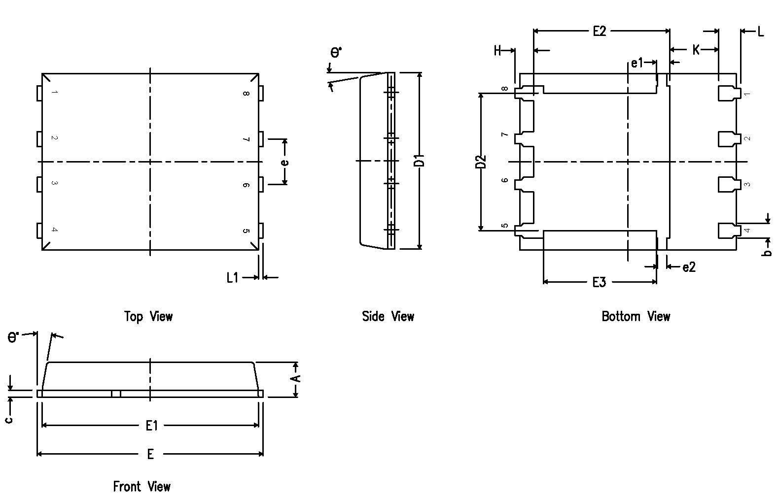
7.1 Q5A Package Dimensions

| DIM | MILLIMETERS | ||
|---|---|---|---|
| MIN | NOM | MAX | |
| A | 0.90 | 1.00 | 1.10 |
| b | 0.33 | 0.41 | 0.51 |
| c | 0.20 | 0.25 | 0.34 |
| D1 | 4.80 | 4.90 | 5.00 |
| D2 | 3.61 | 3.81 | 4.02 |
| E | 5.90 | 6.00 | 6.10 |
| E1 | 5.70 | 5.75 | 5.80 |
| E2 | 3.38 | 3.58 | 3.78 |
| E3 | 3.03 | 3.13 | 3.23 |
| e | 1.17 | 1.27 | 1.37 |
| e1 | 0.27 | 0.37 | 0.47 |
| e2 | 0.15 | 0.25 | 0.35 |
| H | 0.41 | 0.56 | 0.71 |
| K | 1.10 | ||
| L | 0.51 | 0.61 | 0.71 |
| L1 | 0.06 | 0.13 | 0.20 |
| θ | 0° | 12° | |
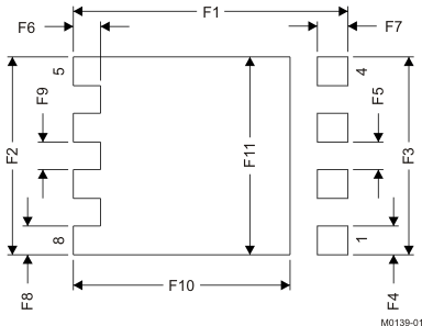
7.2 Recommended PCB Pattern

| DIM | MILLIMETERS | INCHES | ||
|---|---|---|---|---|
| MIN | MAX | MIN | MAX | |
| F1 | 6.205 | 6.305 | 0.244 | 0.248 |
| F2 | 4.46 | 4.56 | 0.176 | 0.18 |
| F3 | 4.46 | 4.56 | 0.176 | 0.18 |
| F4 | 0.65 | 0.7 | 0.026 | 0.028 |
| F5 | 0.62 | 0.67 | 0.024 | 0.026 |
| F6 | 0.63 | 0.68 | 0.025 | 0.027 |
| F7 | 0.7 | 0.8 | 0.028 | 0.031 |
| F8 | 0.65 | 0.7 | 0.026 | 0.028 |
| F9 | 0.62 | 0.67 | 0.024 | 0.026 |
| F10 | 4.9 | 5 | 0.193 | 0.197 |
| F11 | 4.46 | 4.56 | 0.176 | 0.18 |
For recommended circuit layout for PCB designs, see application note SLPA005 – Reducing Ringing Through PCB Layout Techniques.
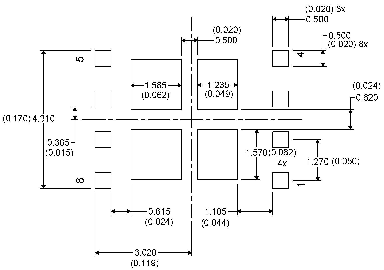
7.3 Recommended Stencil Opening

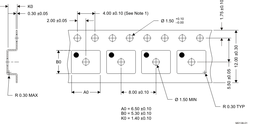
7.4 Q5A Tape and Reel Information

Notes:
- 10-sprocket hole-pitch cumulative tolerance ±0.2
- Camber not to exceed 1 mm in 100 mm, noncumulative over 250 mm
- Material: black static-dissipative polystyrene
- All dimensions are in mm (unless otherwise specified)
- A0 and B0 measured on a plane 0.3 mm above the bottom of the pocket