-
CSD23203W –8-V P-Channel NexFET Power MOSFET
Package Options
Refer to the PDF data sheet for device specific package drawings
Mechanical Data (Package|Pins)
- YZC|6
Thermal pad, mechanical data (Package|Pins)
Orderable Information
CSD23203W –8-V P-Channel NexFET Power MOSFET
1 Features
- Ultra-Low Qg and Qgd
- Low RDS(on)
- Small Footprint
- Low Profile 0.62-mm Height
- Lead Free
- RoHS Compliant
- Halogen Free
- CSP 1-mm × 1.5-mm Wafer Level Package
2 Applications
- Battery Management
- Load Switch
- Battery Protection
3 Description
This 16.2-mΩ, –8-V, P-Channel device is designed to deliver the lowest on-resistance and gate charge in a small 1 × 1.5 mm outline with excellent thermal characteristics in an ultra-low profile.
Product Summary
| TA = 25°C | TYPICAL VALUE | UNIT | ||
|---|---|---|---|---|
| VDS | Drain-to-Source Voltage | –8 | V | |
| Qg | Gate Charge Total (–4.5 V) | 4.9 | nC | |
| Qgd | Gate Charge Gate-to-Drain | 0.6 | nC | |
| RDS(on) | Drain-to-Source On-Resistance |
VGS = –1.8 V | 35 | mΩ |
| VGS = –2.5 V | 22 | mΩ | ||
| VGS = –4.5 V | 16.2 | mΩ | ||
| VGS(th) | Voltage Threshold | –0.8 | V | |
Device Information(1)
| DEVICE | QTY | MEDIA | PACKAGE | SHIP |
|---|---|---|---|---|
| CSD23203W | 3000 | 7-Inch Reel | 1.00-mm × 1.50-mm Wafer Level Package |
Tape and Reel |
| CSD23203WT | 250 | 7-Inch Reel |
- For all available packages, see the orderable addendum at the end of the data sheet.
Absolute Maximum Ratings
| TA = 25°C | VALUE | UNIT | |
|---|---|---|---|
| VDS | Drain-to-Source Voltage | –8 | V |
| VGS | Gate-to-Source Voltage | –6 | V |
| ID | Continuous Drain Current(1) | –3 | A |
| IDM | Pulsed Drain Current(2) | –54 | A |
| PD | Power Dissipation | 0.75 | W |
| TJ,
Tstg |
Operating Junction, Storage Temperature |
–55 to 150 | °C |
- Device operating at a temperature of 105ºC.
- Typ RθJA = 170°C/W, pulse width ≤ 100 μs, duty cycle ≤ 1%.
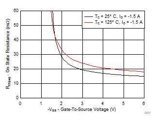
RDS(on) vs VGS |
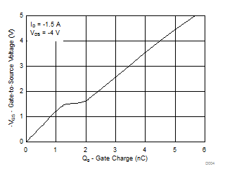
Gate Charge |
5 Specifications
5.1 Electrical Characteristics
TA = 25°C (unless otherwise stated)| PARAMETER | TEST CONDITIONS | MIN | TYP | MAX | UNIT | ||
|---|---|---|---|---|---|---|---|
| STATIC CHARACTERISTICS | |||||||
| BVDSS | Drain-to-source voltage | VGS = 0 V, ID = –250 μA | –8 | V | |||
| IDSS | Drain-to-source leakage current | VGS = 0 V, VDS = –6.4 V | –1 | μA | |||
| IGSS | Gate-to-source leakage current | VDS = 0 V, VGS = –6 V | –100 | nA | |||
| VGS(th) | Gate-to-source threshold voltage | VDS = VGS, ID = –250 μA | -0.6 | –0.8 | –1.1 | V | |
| RDS(on) | Drain-to-source on-resistance | VGS = –1.8 V, ID = –1.5 A | 35 | 53 | mΩ | ||
| VGS = –2.5 V, ID = –1.5 A | 22 | 26.5 | mΩ | ||||
| VGS = –4.5 V, ID = –1.5 A | 16.2 | 19.4 | mΩ | ||||
| gƒs | Transconductance | VDS = –0.8 V, ID = –1.5 A | 14 | S | |||
| DYNAMIC CHARACTERISTICS | |||||||
| CISS | Input capacitance | VGS = 0 V, VDS = –4 V, ƒ = 1 MHz | 703 | 914 | pF | ||
| COSS | Output capacitance | 391 | 508 | pF | |||
| CRSS | Reverse transfer capacitance | 133 | 172 | pF | |||
| Qg | Gate charge total (–4.5 V) | VDS = –4 V, ID = –1.5 A | 4.9 | 6.3 | nC | ||
| Qgd | Gate charge gate-to-drain | 0.6 | nC | ||||
| Qgs | Gate charge gate-to-source | 1.3 | nC | ||||
| Qg(th) | Gate charge at Vth | 0.6 | nC | ||||
| QOSS | Output charge | VDS = –4 V, VGS = 0 V | 1.9 | nC | |||
| td(on) | Turnon delay time | VDS = –4 V, VGS = –4.5 V, ID = –1.5 A RG = 10 Ω |
14 | ns | |||
| tr | Rise time | 12 | ns | ||||
| td(off) | Turnoff delay time | 58 | ns | ||||
| tƒ | Fall time | 27 | ns | ||||
| DIODE CHARACTERISTICS | |||||||
| VSD | Diode forward voltage | IS = –1.5 A, VGS = 0 V | –0.75 | –1 | V | ||
| Qrr | Reverse recovery charge | VDS= –4.7 V, IF = –1.5 A di/dt = 100 A/μs |
6.1 | nC | |||
| trr | Reverse recovery time | 21 | ns | ||||
5.2 Thermal Information
TA = 25°C (unless otherwise stated)| THERMAL METRIC | MIN | TYP | MAX | UNIT | |
|---|---|---|---|---|---|
| RθJA | Junction-to-ambient thermal resistance(1) | 170 | °C/W | ||
| Junction-to-ambient thermal resistance(2) | 55 | ||||
 |
Typ RθJA = 55°C/W when mounted on 1 in2 of 2-oz Cu. |
 |
Typ RθJA = 170°C/W when mounted on minimum pad area of 2-oz Cu. |
5.3 Typical MOSFET Characteristics
TA = 25°C (unless otherwise stated)
SPACE


| ID = –1.5 A | VDS = –4 V | |

| ID = –250 µA | ||

| ID = –1.5 A | ||

| Single Pulse, Typical RθJA = 170°C/W | ||

| VDS = –5 V | ||


6 Device and Documentation Support
6.1 Receiving Notification of Documentation Updates
To receive notification of documentation updates, navigate to the device product folder on ti.com. In the upper right corner, click on Alert me to register and receive a weekly digest of any product information that has changed. For change details, review the revision history included in any revised document.
6.2 Community Resources
The following links connect to TI community resources. Linked contents are provided "AS IS" by the respective contributors. They do not constitute TI specifications and do not necessarily reflect TI's views; see TI's Terms of Use.
-
TI E2E™ Online Community TI's Engineer-to-Engineer (E2E) Community. Created to foster collaboration among engineers. At e2e.ti.com, you can ask questions, share knowledge, explore ideas and help solve problems with fellow engineers.
-
Design Support TI's Design Support Quickly find helpful E2E forums along with design support tools and contact information for technical support.
6.3 Trademarks
E2E is a trademark of Texas Instruments.
All other trademarks are the property of their respective owners.
6.4 Electrostatic Discharge Caution

These devices have limited built-in ESD protection. The leads should be shorted together or the device placed in conductive foam during storage or handling to prevent electrostatic damage to the MOS gates.
6.5 Glossary
SLYZ022 — TI Glossary.
This glossary lists and explains terms, acronyms, and definitions.
