DATA SHEET
CSD75207W15 Dual P-Channel NexFET Power MOSFET
1 Features
- Dual P-Channel MOSFETs
- Common Source Configuration
- Small Footprint 1.5-mm × 1.5-mm
- Gate-Source Voltage Clamp
- Gate ESD Protection >4 kV
- HBM JEDEC standard JESD22-A114
- Pb and Halogen Free
- RoHS Compliant
2 Applications
- Battery Management
- Battery Protection
- Load and Input Switching
3 Description
The CSD75207W15 device is designed to deliver the lowest on-resistance and gate charge in the smallest outline possible with excellent thermal characteristics in an ultra-low profile. Low on-resistance coupled with the small footprint and low profile make the device ideal for battery-operated space-constrained applications. The device has also been awarded with U.S. patents 7952145, 7420247, 7235845, and 6600182.

Product Summary
| TA = 25°C | TYPICAL VALUE | UNIT | ||
|---|---|---|---|---|
| VD1D2 | Drain-to-Drain Voltage | –20 | V | |
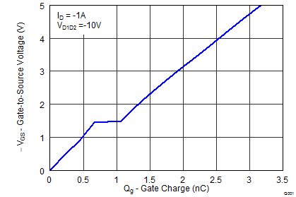
| Qg | Gate Charge Total (–4.5 V) | 2.9 | nC | |
| Qgd | Gate Charge Gate to Drain | 0.4 | nC | |
| RD1D2(on) | Drain-to-Drain On Resistance | VGS = –1.8 V | 119 | mΩ |
| VGS = –2.5 V | 64 | mΩ | ||
| VGS = –4.5 V | 45 | mΩ | ||
| VGS(th) | Threshold Voltage | –0.8 | V | |
Ordering Information(1)
| Device | Package | Media | Qty | Ship |
|---|---|---|---|---|
| CSD75207W15 | 1.5-mm × 1.5-mm Wafer Level Package | 7-Inch Reel | 3000 | Tape and Reel |
- For all available packages, see the orderable addendum at the end of the data sheet.
Absolute Maximum Ratings
| TA = 25°C | VALUE | UNIT | |
|---|---|---|---|
| VD1D2 | Drain-to-Drain Voltage | –20 | V |
| VGS | Gate-to-Source Voltage | –6.0 | V |
| ID1D2 | Continuous Drain to Drain Current(1)(2) | –3.9 | A |
| Pulsed Drain to Drain Current, TC = 25°C(3) |
–24 | A | |
| IS | Continuous Source Pin Current | –1.2 | A |
| Pulsed Source Pin Current(3) | –15 | A | |
| IG | Continuous Gate Clamp Current | –0.5 | A |
| Pulsed Gate Clamp Current(3) | –7 | A | |
| PD | Power Dissipation(1) | 0.7 | W |
| TJ, Tstg |
Operating Junction and Storage Temperature Range |
–55 to 150 | °C |
Top View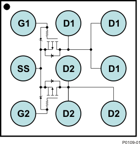 |
RD1D2(on) vs VGS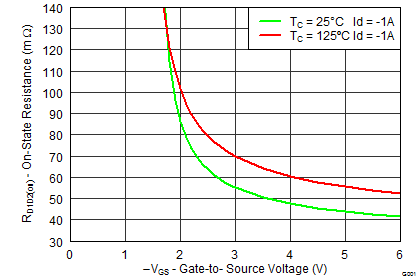 |
5 Specifications
5.1 Electrical Characteristics
(TA = 25°C unless otherwise stated). Specifications and graphs are Per MOSFET unless otherwise stated. Drain to Drain measurements are done with both MOSFETs in series (common source configuration.| PARAMETER | TEST CONDITIONS | MIN | TYP | MAX | UNIT | ||
|---|---|---|---|---|---|---|---|
| STATIC CHARACTERISTICS | |||||||
| BVD1D2 | Drain-to-Drain Voltage | VGS = 0 V, ID1D2 = –250 μA | –20 | V | |||
| BVGSS | Gate-to-Source Voltage | VD1D2 = 0 V, IG = -250 μA | –6 | V | |||
| IDDS | Drain-to-Drain Leakage Current | VGS = 0 V, VD1D2 = –16 V | –1 | μA | |||
| IGSS | Gate-to-Source Leakage Current | VD1D2 = 0 V, VGS = –6 V | –100 | nA | |||
| VGS(th) | Gate-to-Source Threshold Voltage | VD1D2 = VGS, IDS = –250 μA | –0.6 | –0.8 | –1.1 | V | |
| RD1D2(on) | Drain-to-Drain On-Resistance | VGS = –1.8 V, ID1D2 = –1 A | 119 | 162 | mΩ | ||
| VGS = –2.5 V, ID1D2 = –1 A | 64 | 77 | mΩ | ||||
| VGS = –4.5 V, ID1D2 = –1 A | 45 | 54 | mΩ | ||||
| gfs | Transconductance | VD1D2 = –10 V, ID1D2 = –1 A | 6.2 | S | |||
| DYNAMIC CHARACTERISTICS | |||||||
| CISS | Input Capacitance | VGS = 0 V, VD1D2 = –10 V, ƒ = 1 MHz |
458 | 595 | pF | ||
| COSS | Output Capacitance | 225 | 293 | pF | |||
| CRSS | Reverse Transfer Capacitance | 10.4 | 13.5 | pF | |||
| Rg | Series Gate Resistance | 27 | Ω | ||||
| Qg | Gate Charge Total (–4.5 V) | VD1D2 = –10 V, ID1D2 = –1 A |
2.9 | 3.7 | nC | ||
| Qgd | Gate Charge – Gate to Drain | 0.4 | nC | ||||
| Qgs | Gate Charge – Gate to Source | 0.7 | nC | ||||
| Qg(th) | Gate Charge at Vth | 0.4 | nC | ||||
| QOSS | Output Charge | VD1D2 = –9.5 V, VGS = 0 V | 3.1 | nC | |||
| td(on) | Turn On Delay Time | VD1D2 = –10 V, VGS = –4.5 V, ID1D2 = –1 A, RG = 30 Ω |
12.8 | ns | |||
| tr | Rise Time | 8.6 | ns | ||||
| td(off) | Turn Off Delay Time | 32.1 | ns | ||||
| tf | Fall Time | 16.0 | ns | ||||
| DIODE CHARACTERISTICS | |||||||
| VSD | Diode Forward Voltage | ID1D2 = –1 A, VGS = 0 V | –0.8 | –1 | V | ||
| Qrr | Reverse Recovery Charge | Vdd = –10 V, IF = –1 A, di/dt = 200 A/μs | 10.5 | nC | |||
| trr | Reverse Recovery Time | Vdd = –10 V, IF = –1 A, di/dt = 200 A/μs | 23 | ns | |||
5.2 Thermal Information
(TA = 25°C unless otherwise stated)| THERMAL METRIC | TYPICAL VALUE | UNIT | |||
|---|---|---|---|---|---|
| R θJA | Junction-to-Ambient Thermal Resistance(1)(3) | 70 | °C/W | ||
| Junction-to-Ambient Thermal Resistance (2)(3) | 165 | ||||
(1) Device mounted on FR4 material with Minimum Cu mounting area.
(2) Device mounted on FR4 material with 1-inch2 of Cu (2 oz).
(3) Measured with both devices biased in a parallel condition.
 |
Typ RθJA = 70°C/W when mounted on 1-inch2 of 2 oz. Cu. |
 |
Typ RθJA = 165°C/W when mounted on minimum pad area of 2-oz. Cu. |
5.3 Typical MOSFET Characteristics
(TA = 25°C unless otherwise stated)