SLPS642 April 2017 CSD87313DMS
PRODUCTION DATA.
- 1Features
- 2Applications
- 3Description
- 4Revision History
- 5 Specifications
- 6Device and Documentation Support
- 7Mechanical, Packaging, and Orderable Information
Package Options
Refer to the PDF data sheet for device specific package drawings
Mechanical Data (Package|Pins)
- DMS|8
Thermal pad, mechanical data (Package|Pins)
Orderable Information
1 Features
- Low-Source-to-Source On Resistance
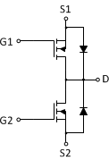
- Dual Common Drain N-Channel MOSFETs
- Optimized for 5-V Gate Drive
- Low Qg and Qgd
- Low-Thermal Resistance
- Avalanche Rated
- Lead-Free Terminal Plating
- RoHS Compliant
- Halogen Free
- SON 3.3-mm × 3.3-mm Plastic Package
2 Applications
- USB Type-C™ and Power Delivery (PD) VBus Protection
- Battery Protection
- Load Switch
3 Description
The CSD87313DMS is a 30-V common drain, dual N-channel device designed for USB Type-C/PD and battery protection. This SON 3.3-mm × 3.3-mm device has low-source-to-source on resistance that minimizes losses and offers low-component count for space constrained applications.
Schematic

Product Summary
| TA = 25°C | VALUE | UNIT | ||
|---|---|---|---|---|
| VS1S2 | Source1-to-Source2 Voltage | 30 | V | |
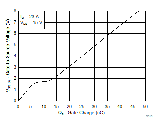
| Qg | Gate Charge Total (4.5 V) | 28 | nC | |
| Qgd | Gate Charge Gate-to-Drain | 6.0 | nC | |
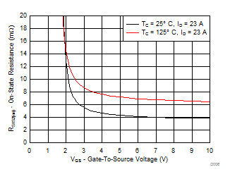
| RS1S2(on) | Max Source1-to-Source2 On Resistance | VGS = 2.5 V | 9.6 | mΩ |
| VGS = 4.5 V | 5.5 | |||
| VGS(th) | Threshold Voltage | 0.9 | V | |
Device Information(1)
| DEVICE | QTY | MEDIA | PACKAGE | SHIP |
|---|---|---|---|---|
| CSD87313DMS | 2500 | 13-Inch Reel | SON 3.30-mm × 3.30-mm Plastic Package |
Tape and Reel |
| CSD87313DMST | 250 | 7-Inch Reel |
- For all available packages, see the orderable addendum at the end of the data sheet.
Absolute Maximum Ratings
| TA = 25°C unless otherwise stated | VALUE | UNIT | |
|---|---|---|---|
| VS1S2 | Source1-to-Source2 Voltage | 30 | V |
| VGS | Gate-to-Source Voltage(1) | ±10 | V |
| IS1S2 | Continuous Source Current(2) | 17 | A |
| ISM | Pulsed Source Current, TA = 25°C(2)(3) | 120 | A |
| PD | Power Dissipation(2) | 2.7 | W |
| Power Dissipation(4) | 1 | ||
| TJ, Tstg | Operating Junction, Storage Temperature |
–55 to 150 | °C |
| EAS | Avalanche Energy, Single Pulse, ID = 37 A, L = 0.1 mH, RG = 25 Ω |
67 | mJ |
- VG1S1 should not exceed ±10 V and VG2S2 should not exceed ±10 V.
- Typical RθJA = 45°C/W when mounted on a 1-in2 (6.45-cm2), 2-oz (0.071-mm) thick Cu pad on a 0.06-in (1.52-mm) thick FR4 PCB.
- Duty cycle ≤ 2%, pulse duration ≤ 300 µs.
- Typical RθJA = 125°C/W on a minimum 2-oz Cu pad.
RS1S2(ON) vs VGS |
Gate Charge |