-
CSD95379Q3M Synchronous Buck NexFET Power Stage
Package Options
Mechanical Data (Package|Pins)
- DNS|10
Thermal pad, mechanical data (Package|Pins)
Orderable Information
CSD95379Q3M Synchronous Buck NexFET Power Stage
1 Features
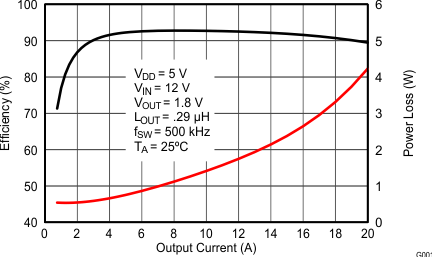
- 92.5% System Efficiency at 12 A
- Ultra-Low Power Loss of 1.8 W at 12 A
- Max Rated Continuous Current of 20 A and Peak Current of 45 A
- High-Frequency Operation (up to 2 MHz)
- High-Density SON 3.3-mm × 3.3-mm Footprint
- Ultra-Low Inductance Package
- System Optimized PCB Footprint
- Low Quiescent (LQ) and Ultra-Low Quiescent (ULQ) Current Mode
- 3.3-V and 5-V PWM Signal Compatible
- Diode Emulation Mode with FCCM
- Tri-State PWM Input
- Integrated Bootstrap Diode
- Shoot-Through Protection
- RoHS Compliant – Lead-Free Terminal Plating
- Halogen Free
2 Applications
- NVDC Notebook and Ultrabook PCs
- Tablets
- Point of Load Synchronous Buck in Networking, Telecom, and Computing Systems
3 Description
The CSD95379Q3M NexFET™ power stage is a highly optimized design for use in high-power, high-density synchronous buck converters. This product integrates the driver IC and NexFET technology to complete the power stage switching function. The driver IC has a built-in selectable diode emulation function that enables DCM operation to improve light load efficiency. In addition, the driver IC supports ULQ mode that enables Connected Standby for Windows® 8. With the PWM input in tri-state, quiescent current is reduced to 130 µA, with immediate response. When SKIP# is held at tri-state, the current is reduced to 8 µA (typically 20 µs is required to resume switching). This combination produces high-current, high-efficiency, and high-speed switching capability in a small 3.3-mm × 3.3-mm outline package. In addition, the PCB footprint has been optimized to help reduce design time and simplify the completion of the overall system design.
Device Information(1)
| DEVICE | MEDIA | QTY | PACKAGE | SHIP | |
|---|---|---|---|---|---|
| CSD95379Q3M | 13-Inch Reel | 2500 | SON 3.3-mm × 3.3-mm Plastic Package |
Tape and Reel | |
| CSD95379Q3MT | 7-Inch Reel | 250 | |||
.
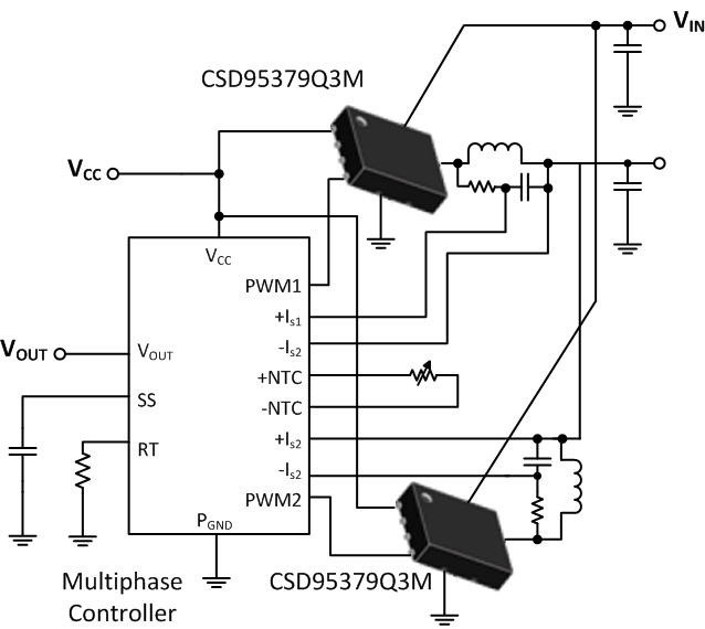
Application Diagram
Typical Power Stage Efficiency and Power Loss
4 Revision History
Changes from C Revision (November 2014) to D Revision
- Added minimum value for ƒSW in the Recommended Operating Conditions tableGo
- Added Receiving Notification of Documentation Updates and Community Resources to Device and Documentation Support sectionGo
Changes from B Revision (November 2014) to C Revision
- Added footnote 1 under Recommended Operating ConditionsGo
Changes from A Revision (August 2014) to B Revision
- Changed device status to production data.Go
Changes from * Revision (April 2014) to A Revision
- Increased VIN from 14.5 V to 16 VGo
5 Pin Configuration and Functions

Pin Functions
| PIN | DESCRIPTION | |
|---|---|---|
| NAME | NUMBER | |
| SKIP# | 1 | This pin enables the Diode Emulation function. When this pin is held low, Diode Emulation Mode is enabled for the sync FET. When SKIP# is high, the CSD95379Q3M operates in Forced Continuous Conduction Mode. A tri-state voltage on SKIP# puts the driver into a very-low power state. |
| VDD | 3 | Supply voltage to gate drivers and internal circuitry. |
| PGND | 4 | Power ground. Needs to be connected to pin 11 on the PCB. |
| VSW | 5 | Voltage switching node – pin connection to output inductor. |
| VIN | 6 | Input voltage pin. Connect input capacitors to close this pin. |
| BOOT_R | 7 | Bootstrap capacitor connection. Connect a minimum 0.1-µF, 16-V X5R, ceramic capacitor from BOOT to BOOT_R pins. The bootstrap capacitor provides the charge to turn on the control FET. The bootstrap diode is integrated. |
| BOOT | 8 | |
| PWM | 10 | Pulse-width-modulated tri-state input from external controller. Logic low sets control FET gate low and sync FET gate high. Logic high sets control FET gate high and sync FET gate low. Open or High Z sets both MOSFET gates low if greater than the tri-state shutdown hold-off time (T3HT). |
| PGND | 11 | Power ground. Needs to be connected to pin 4 on the PCB. |
6 Specifications
6.1 Absolute Maximum Ratings(1)
TA = 25°C (unless otherwise noted)| MIN | MAX | UNIT | ||
|---|---|---|---|---|
| VIN to PGND | –0.3 | 20 | V | |
| VSW to PGND , VIN to VSW | –0.3 | 20 | V | |
| VSW to PGND, VIN to VSW (<10 ns) | –7 | 23 | V | |
| VDD to PGND | –0.3 | 6 | V | |
| PWM, SKIP# to PGND | –0.3 | 6 | V | |
| BOOT to PGND | –0.3 | 25 | V | |
| BOOT to PGND (<10 ns) | –2 | 28 | V | |
| BOOT to BOOT_R | –0.3 | 6 | V | |
| PD | Power dissipation | 6 | W | |
| TJ | Operating temperature | –40 | 150 | °C |
| Tstg | Storage temperature | –55 | 150 | °C |
6.2 ESD Ratings
| VALUE | UNIT | ||||
|---|---|---|---|---|---|
| V(ESD) | Electrostatic discharge | Human-body model (HBM), per ANSI/ESDA/JEDEC JS-001, all pins (1) | ±2000 | V | |
| Charged-device model (CDM), per JEDEC specification JESD22-C101, all pins(2) | ±500 | ||||
6.3 Recommended Operating Conditions
TA = 25° (unless otherwise noted)| MIN | MAX | UNIT | |||
|---|---|---|---|---|---|
| VDD | Gate drive voltage | 4.5 | 5.5 | V | |
| VIN | Input supply voltage(1) | 16 | V | ||
| IOUT | Continuous output current | VIN = 12 V, VDD = 5 V, VOUT = 1.8 V, ƒSW = 500 kHz, LOUT = 0.29 µH(2) |
20 | A | |
| IOUT-PK | Peak output current(3) | 45 | A | ||
| ƒSW | Switching frequency | CBST = 0.1 µF (min) | 25 | 2000 | kHz |
| On time duty cycle | 85% | ||||
| Minimum PWM on time | 40 | ns | |||
| Operating temperature | –40 | 125 | °C | ||
6.4 Thermal Information
TA = 25°C (unless otherwise noted)| THERMAL METRIC | MIN | TYP | MAX | UNIT | |
|---|---|---|---|---|---|
| RθJC(top) | Junction-to-case thermal resistance (top of package)(1) | 22.8 | °C/W | ||
| RθJB | Junction-to-board thermal resistance(2) | 2.5 | |||
0.06-in (1.52-mm) thick FR4 board.
6.5 Electrical Characteristics
TA = 25°C, VDD = POR to 5.5 V (unless otherwise noted)| PARAMETER | TEST CONDITIONS | MIN | TYP | MAX | UNIT | |
|---|---|---|---|---|---|---|
| PLOSS | ||||||
| Power loss(1) | VIN = 12 V, VDD = 5 V, VOUT = 1.8 V, IOUT = 12 A, ƒSW = 500 kHz, LOUT = 0.29 µH , TJ = 25°C |
1.8 | W | |||
| Power loss(2) | VIN = 12 V, VDD = 5 V, VOUT = 1.8 V, IOUT = 12 A, ƒSW = 500 kHz, LOUT = 0.29 µH , TJ = 125°C |
2.3 | W | |||
| VIN | ||||||
| IQ | VIN quiescent current | PWM = float, VIN = 14.5 V, VDD = 5 V | 1 | µA | ||
| VDD | ||||||
| IDD | Standby supply current | PWM = float, VSKIP# = VDD or 0 V | 130 | µA | ||
| VSKIP# = float | 8 | |||||
| IDD | Operating supply current | PWM = 50% duty cycle, ƒSW = 500 kHz | 5.5 | mA | ||
| POWER-ON RESET AND UNDERVOLTAGE LOCKOUT | ||||||
| VDD rising | Power-on reset | 4.15 | V | |||
| VDD falling | UVLO | 3.7 | V | |||
| Hysteresis | 0.2 | mV | ||||
| PWM AND SKIP# I/O SPECIFICATIONS | ||||||
| RI | Input impedance | Pullup to VDD | 1700 | kΩ | ||
| Pulldown to GND | 800 | |||||
| VIH | Logic level high | 2.65 | V | |||
| VIL | Logic level low | 0.6 | V | |||
| VIH | Hysteresis | 0.2 | V | |||
| VTS | Tri-state voltage | 1.3 | 2 | V | ||
| tHOLD(off1) | Tri-state activation time (falling) PWM(2) | 60 | ns | |||
| tHOLD(off2) | Tri-state activation time (rising) PWM(2) | 60 | ns | |||
| tTSKF | Tri-state activation time (falling) SKIP#(2) | 1 | ns | |||
| tTSKR | Tri-state activation time (rising) SKIP#(2) | 1 | ns | |||
| t3RD(PWM) | Tri-state exit time PWM(2) | 100 | ns | |||
| t3RD(SKIP#) | Tri-state exit time SKIP#(2) | 50 | us | |||
| BOOTSTRAP SWITCH | ||||||
| VFBOOT | Forward voltage | Measured from VDD to VBOOT, IF = 20 mA | 120 | 240 | mV | |
| IRBOOT | Reverse leakage(1) | VBOOT – VDD = 25 V | 2 | µA | ||
6.6 Typical Characteristics
TJ = 125°C, unless stated otherwise. The Typical CSD95379Q3M system characteristic curves are based on measurements made on a PCB design with dimensions of 4 in (W) × 3.5 in (L) × 0.062 in (T) and 6 copper layers of 1-oz copper thickness. See the Application and Implementation section for detailed explanation.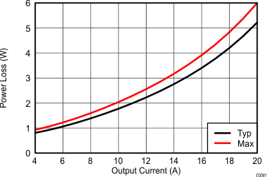
| VIN = 12 V | VDD = 5 V | VOUT = 1.8 V |
| ƒSW = 500 kHz | LOUT = 0.29 µH |
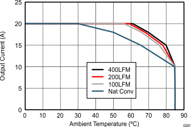
| VIN = 12 V | VDD = 5 V | VOUT = 1.8 V |
| ƒSW = 500 kHz | LOUT = 0.29 µH |
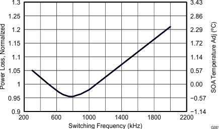
| VIN = 12 V | VDD = 5 V | VOUT = 1.8 V |
| LOUT = 0.29 µH | IOUT = 18 A |
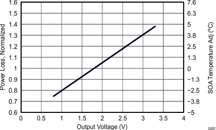
| VIN = 12 V | VDD = 5 V | ƒSW = 500 kHz |
| LOUT = 0.29 µH | IOUT = 18 A |
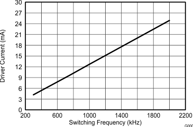
| VIN = 12 V | VDD = 5 V | VOUT = 1.8 V | ||
| LOUT = 0.29 µH | IOUT = 18 A |
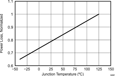
| VIN = 12 V | VDD = 5 V | VOUT = 1.8 V |
| ƒSW = 500 kHz | LOUT = 0.29 µH |
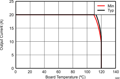
| VIN = 12 V | VDD = 5 V | VOUT = 1.8 V |
| ƒSW = 500 kHz | LOUT = 0.29 µH |
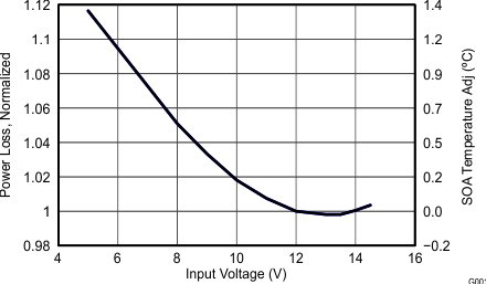
| VDD = 5 V | VOUT = 1.8 V | LOUT = 0.29 µH |
| ƒSW = 500 kHz | IOUT = 18 A |
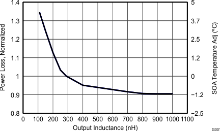
| VIN = 12 V | VDD = 5 V | VOUT = 1.8 V |
| ƒSW = 500 kHz | IOUT = 18 A |