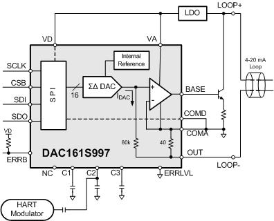
The DAC161S997 is a very low power 16-bit ΣΔ digital-to-analog converter (DAC) for transmitting an analog output current over an industry standard 4-20 mA current loop. The DAC161S997 has a simple 4-wire SPI for data transfer and configuration of the DAC functions. To reduce power and component count in compact loop-powered applications, the DAC161S997 contains an internal ultra-low power voltage reference and an internal oscillator. The low power consumption of the DAC161S997 results in additional current being available for the remaining portion of the system. The loop drive of the DAC161S997 interfaces to a Highway Addressable Remote Transducer (HART) modulator, allowing injection of FSK modulated digital data into the 4-20 mA current loop. This combination of specifications and features makes the DAC161S997 ideal for 2- and 4-wire industrial transmitters. The DAC161S997 is available in a 16-pin 4-mm × 4-mm WQFN package and is specified over the extended industrial temperature range of –40°C to +105°C.
PART NUMBER | PACKAGE | BODY SIZE (NOM) |
---|---|---|
DAC161S997 | WQFN (16) | 4.00 mm x 4.00 mm |
Changes from * Revision ( June 2013) to A Revision
PIN | TYPE(1) | DESCRIPTION | |
---|---|---|---|
NAME | NO. | ||
BASE | 16 | A | External NPN base drive |
COMA | 1 | P | Analog-block negative supply rail (local COMMON) |
COMD | 2 | P | Digital-block negative supply rail (local COMMON) |
CSB | 6 | I | SPI chip select |
C1 | 14 | A | External capacitor |
C2 | 13 | A | External capacitor, HART input |
C3 | 12 | A | External capacitor |
EERB | 7 | O | Error flag output, open drain, active LOW |
ERRLVL | 10 | I | Sets output-current level at power up and under-error conditions. |
NC | 11 | – | Do not connect to this pin. |
OUT | 9 | A | Loop output current source output |
SCLK | 4 | I | SPI clock input |
SDI | 5 | I | SPI data input |
SDO | 8 | O | SPI data output |
VA | 15 | P | Analog-block positive supply rail |
VD | 3 | P | Digital-block positive supply rail. |
DAP | DAP | P | Die attach pad. Connect directly to local COMMON (COMA, COMD). |
MIN | MAX | UNIT | ||
---|---|---|---|---|
Supply voltage (VA, VD to COMA, COMD) | –0.3 | 6 | V | |
Voltage between any two pins(2) | 6 | V | ||
Current IN or OUT of any pin — except OUT pin(3) | 5 | mA | ||
Output current at OUT | 50 | mA | ||
Junction Temperature | 150 | °C | ||
Operating Temperature | –40 | 105 | °C | |
Storage temperature, Tstg | –65 | 150 | °C |
VALUE | UNIT | |||
---|---|---|---|---|
V(ESD) | Electrostatic discharge | Human-body model (HBM), per ANSI/ESDA/JEDEC JS-001(1)(4) | 2000 | V |
MIN | MAX | UNIT | ||
---|---|---|---|---|
BASE load to COMA | 0 | 15 | pF | |
(COMA - COMD) | 0 | V | ||
OUT load to COMA | none | |||
(VA - VD) | 0 | V | ||
VA, VDD | Supply voltage | 2.7 | 3.6 | V |
TA | Temperature | –40 | 105 | °C |
DAC161S997 | UNIT | |||||
---|---|---|---|---|---|---|
WQFN | ||||||
16 PINS | ||||||
RθJA | Package thermal impedance(1) | 35 | °C/W |
PARAMETER | TEST CONDITIONS | MIN(7) | TYP | MAX(7) | UNIT | |
---|---|---|---|---|---|---|
POWER SUPPLY | ||||||
VA, VD | Supply voltage | VA = VD -40°C ≤ TA ≤ 105°C |
2.7 | 3.6 | V | |
VA supply current | DACCODE = 0x0200(1) | 43 | µA | |||
VD supply current | 57 | µA | ||||
ICC | Total supply current | 100 | 125 | µA | ||
DC ACCURACY | ||||||
N | Resolution | 16 | bits | |||
INL | Integral non-linearity(6) | 0x2AAA < DACCODE < 0xD555 (4 mA < ILOOP < 20 mA) |
–1.5 | 2.6 | µA | |
DNL | Differential non-linearity | see (2) | –0.2 | 0.2 | µA | |
TUE | Total unadjusted error | 0x2AAA < DACCODE < 0xD555 | 0.01 | %FS | ||
OE | Offset error | see (3) | –7.86 | 0.84 | 7.86 | µA |
ΔOE | Offset error temperature coefficient | -40°C ≤ TA ≤ 105°C | 0.48 | ppmFS/°C | ||
GE | Gain error | see (4) | 0.007 | %FS | ||
ΔGE | Gain error temperature coefficient | -40°C ≤ TA ≤ 105°C | 5 | ppmFS/°C | ||
IERRL | LOW ERROR current | ERR_LOW = default | 3.36 | 3.375 | 3.39 | mA |
IERRH | HIGH ERROR current | ERR_HIGH = default | 21.70 | 21.75 | 21.82 | mA |
LTD | Long term drift — mean shift of 12 mA output current after 1000 hours at 150°C | 90 | ppmFS | |||
LOOP CURRENT OUTPUT (OUT) | ||||||
IOUTMIN | Minimum output current | Tested at DACCODE = 0x01C2(5) | 0.19 | mA | ||
IOUTMAX | Maximum output current | Tested at DACCODE = 0xFFFF | 23.95 | mA | ||
ROUT | Output impedance | 200 | MΩ | |||
COMA to OUT voltage drop | IOUT = 24 mA | 960 | mV | |||
BASE OUTPUT | ||||||
IOUTSC | BASE short circuit output current | BASE forced to COMA potential | 10 | mA | ||
DYNAMIC CHARACTERISTICS | ||||||
Output noise density | 1 kHz | 20 | nA/rtHz | |||
Integrated output noise | 1 Hz to 1 kHz band | 300 | nARMS | |||
INTERNAL TIMER | ||||||
TM | Timeout period | Default setting of TIMEOUT in CONFIG register | 100 | ms | ||
DIGITAL INPUT CHARACTERISTICS | ||||||
IIN | Digital input leakage current | –10 | 10 | µA | ||
VIL | Input low voltage | 0.2 × VD | V | |||
VIH | Input high voltage | 0.7 × VD | V | |||
CIN | Input capacitance | 5 | pF | |||
DIGITAL OUTPUT CHARACTERISTICS | ||||||
VOL | Output Low voltage | Isink = 200 μA | 0.4 | V | ||
VOH | Output HIGH voltage | Isink = 200 μA | 2.6 | V | ||
IOZH, IOZL | TRI-STATE leakage current | –10 | 10 | µA | ||
COUT | TRI-STATE output capacitance | 5 | pF |
MIN | NOM | MAX | UNIT | |||
---|---|---|---|---|---|---|
fCLK | SCLK frequency | 0 | 10 | MHz | ||
tH | SCLK high time | 0.4 / FCLK | 50 | ns | ||
tL | SCLK low time | 0.4 / FCLK | 50 | ns | ||
tCSB | CSB pulse width | 5 | 40 | ns | ||
tCSS | CSB set-up time prior to SCLK rising edge | 5 | ns | |||
tSCH | 24th rising edge of SCLK to CSB rising edge | 15 | ns | |||
tCSH | CSB hold time after the 24th falling edge of SCLK | 6 | 10 | ns | ||
tZSDO | CSB falling edge to SDO valid | 10 | 35 | ns | ||
tSDOZ | CSB rising edge to SDO HiZ | 10 | ns | |||
tDS | SDI data set-up time prior to SCLK rising edge | 10 | ns | |||
tDH | SDI data hold time after SCLK rising edge | 6 | 10 | ns | ||
tDO | SDO output data valid | 30 | ns |
The DAC161S997 is a 16-bit DAC realized as a ∑Δ modulator. The DAC’s output is a current pulse train that is filtered by the on-board low pass RC filter. The final output current is a multiplied copy of the filtered modulator output. This architecture ensures an excellent linearity performance, while minimizing power consumption of the device.
The DAC161S997 eases the design of robust, precise, long-term stable industrial systems by integrating all precision elements on-chip. Only a few external components are needed to realize a low-power, high-precision industrial 4 - 20 mA transmitter.
In case of a fault, or during initial power-up the DAC161S997 will output current in either upper or lower error current band. The choice of band is user selectable via a device pin. The error current value is user programmable via SPI.
By default, the DAC161S997 detects and reports several types of errors.
A loop error occurs when the device is unable to sustain the required output current at OUT pin, typically caused by a drop in loop supply, or an increase in load impedance.
When a loop error occurs, the DAC161S997 changes the OUT-pin current to the value in the ERROR_LOW register, unless the MASK_LOOP_ERR is set to 1. If the MASK_LOOP_ERR is not set, then the device also periodically attempts to reassert the OUT current set in DACCODE by default. If the DACCODE-current output is set, the DAC161S997 then stops reporting a loop error. The interval between reasserts is controlled by the L_RETRY_TIME field in the ERROR_CONFIG register. If the DIS_RETRY_LOOP field in the ERROR_CONFIG register is changed to 1, the device does not periodically check the loop and, instead, only checks the loop after a read of the ERR_STATUS (0x09) register. If the loop error is not resolved, then the loop-error current persists.
When a loop error occurs, the DAC161S997 sets the CURR_LOOP_STATUS and LOOP_STATUS fields in the STATUS register to 1. The LOOP_STATUS field remains set to 1 until the STATUS register is read or the device is reset. If the loop error is cleared, either by the device reasserting the loop current or by changing the OUT current , then the CURR_LOOP_STATUS field clears.
The DAC161S997 expects to receive periodic SPI write commands to ensure that the SPI connection is functioning normally. If no SPI write command occurs within the time indicated by the SPI_TIMEOUT field in the ERROR_CONFIG register, the device reports a SPI timeout error. Note that the SPI write command must be properly formatted to avoid SPI Timeout errors (such as a write command that generates a frame error does not prevent an imminent SPI Timeout error).
SPI Timeout error reporting is inhibited by MASK_SPI_TOUT. SPI Timeout errors are not reported on the loop if MASK_SPI_ERR is set to 1.
Note that a write command to address 0 is not considered a valid write command and will not prevent a SPI Timeout error.
If a SPI write command has an incorrect number of SCLK pulses, the device reports a frame error. The number of SCLK pulses must be an integer and a multiple of 24. A frame error is always reported by ERRB being pulled low. A frame error does not affect the loop current.
By default, the DAC161S997 reports faults to the plant controller by forcing the OUT current into one of two error bands. The error current bands are defined as either greater than 20 mA, or less than 4 mA. Loop errors are reported by setting current of ERR_LOW.
If SPI Timeout Errors are reported on the loop (this is the default; it can be changed by setting the register ERR_CONFIG:MASK_LOOP_ERR), the error band is controlled by the ERRLVL pin. When ERRLVL is tied to the COMD voltage, the ERR_LOW current is the reporting current. If ERRLVL is tied to VD then the ERR_HIGH current is the current-on pin, OUT, if a SPI timeout error occurs.
The exact value of the output current used to indicate fault is dictated by the contents of ERR_HIGH and ERR_LOW registers.
In the case of a conflicting alarm-current setting (such as a loop error and SPI timeout error occurring simultaneously and ERRLVL is tied high), the current-on pin, OUT, is determined by ERR_LOW current.
The DAC161S997 reports errors in 3 different ways, by changing the OUT pin current, pulling the ERRB pin low, and by updating the read-only register STATUS. The reporting on ERRB and OUT pin is customized by setting the ERROR_CONFIG register.
The ERRB pin connects to a GPIO pin on the microcontroller to function as an interrupt if an error occurs.
If a Loop error and a SPI Timeout error occur simultaneously and the device is configured with conflicting error output currents, the OUT pin current reports the Loop Error.
STATUS Register | Loop Reporting | ERRB Reporting | |
---|---|---|---|
Frame Error | Reported in FERR_STS | Not reported | Always reported |
Loop Error | Reported in LOOP_STS and CURR_LOOP_STS | Reported by default unless ERR_CONFIG:MASK_LOOP_ERR is set to 1 | Reported by default unless ERR_CONFIG:DIS_LOOP_ERR_ERRB is set to 1 |
SPI Timeout Error | Reported in SPI_TIMEOUT_ERR | Reported by default unless either ERR_CONFIG:MASK_SPI_ERR or ERR_CONFIG:MASK_SPI_TOUT are set to 1 | Reported by default unless ERR_CONFIG:MASK_SPI_TOUT is set to 1 |
The 4-wire interface is compatible with SPI, QSPI, and MICROWIRE, as well as most DSPs. See the Timing Requirements section for timing information about the read and write sequences. The serial interface is comprised of CSB, SCLK, SDIs and SDO. The DAC161S997 supports both Mode 0 and Mode 3 of the SPI protocol.
A bus transaction is initiated by the falling edge of CSB. When CSB is low, the input data is sampled at the SDI pin by the rising edge of the SCLK. The output data is asserted on the SDO pin at the falling edge of SCLK.
A valid transfer requires an integer multiple of 24 SCLK cycles. If CSB is raised before the 24th rising edge of the SCLK, the transfer aborts and a Frame Error is reported. If CSB is held low after the 24th falling edge of the SCLK and additional SCLK edges occur, the data continues to flow through the FIFO and out the SDO pin. When CSB transitions high, the internal controller decodes the most recent 24 bits that were received before the rising edge of CSB. CSB must transition to high after an integer multiple of 24 clock cycles, otherwise a Frame Error is reported and the transaction is considered invalid. When a valid number of SCLK pulses occur with CSB low, the DAC then performs the requested operation after CSB transitions high.
The acquired data is shifted into an internal 24-bit shift register (MSB first) which is configured as a 24-bit deep FIFO. As the data is being shifted into the FIFO via the SDI pin, the prior contents of the register are being shifted out through the SDO output. While CSB is high, SDO is in a high Z-state. At the falling edge of CSB, SDO presents the MSB of the data present in the shift register. SDO is updated on every subsequent falling edge of SCLK.
NOTE
The first SDO transition will happen on the first falling edge AFTER the first rising edge of SCLK when CSB is low.
The 24 bits of data contained in the FIFO are interpreted as an 8-bit COMMAND word followed by 16-bits of DATA. The general format of the 24-bit data stream is shown in Figure 9. Complete instruction set is tabulated in the Detailed Description section.
SPI write operation is used to change the state of the device. Handshaking does not occur between the master and the slave (DAC161S997), and the master must control the communication on the following inputs: SCLK, CSB, SDI. The format of the data transfer is described in the Serial Interface section.
A write is composed of two sections, 8-bits corresponding to a command and 16-bits of data. A command is simply the address of the desired register to update. Note that some registers are read-only; a write to these registers will have no effect on the device operation and the register contents will not change. The user instruction set is shown in the Detailed Description section.
During power up or device reset, the register contents of all writable registers are set to the listed values in the Detailed Description section.
If the DAC161S997 is used in a highly noisy environment in which SPI errors are potentially an issue, the DAC161S997 supports a more robust protocol (see Optional Protected SPI Writes).
The read operation requires all 4 wires of the SPI interface, which are SCLK, SCB, SDI, and SDO. The simplest READ operation occurs automatically during any valid transaction on the SPI bus because the SDO pin of DAC161S997 always shifts out the contents of the internal FIFO. Therefore the data being shifted in to the FIFO is verified by initiating another transaction and acquiring data at SDO, allowing only for the verification of FIFO contents.
The internal registers are accessed by the user through a register read command. A register read command is formed by setting bit 7 of the command to 1 (effectively ORing with 0x80) with the address of the desired register to be read and sending the resulting 8 bits as the command (see Detailed Description). For example, the register read command of the STATUS register (address 0x05) would be 0x85.
A register read requires two SPI transactions to recover the register data. The first transaction shifts in the register read command; an 8-bits of command byte followed by 16-bits of dummy data. The register read command transfers the contents of the internal register into the FIFO. The second transaction shifts out the FIFO contents; an 8-bit command byte (which is a copy of previous transaction) followed by the register data. The Register Read operation is shown in Figure 10.
The DAC161S997 supports an optional SPI protocol intended to provide robust support against SPI write errors.
When PROTECT_REG_WR is set to 1, all register writes require a subsequent XFER_REG command (a write of 0x00FF to XFER_REG[0x01]) to load the transferred data into the register address (see Figure 11). This requirement provides protection against write errors in an electrically noisy environment.
To minimize the chance of a SPI write error, TI recommends to append a NOP command onto the end of every register write sequence to verify that the XFER_REG is properly executed, as shown in Figure 12.
The XFER_REG command combined with the automatic SDO loopback of the previous SPI write data prevents loading of incorrect data into a register. If the loopback indicates a communication error has occurred (see Figure 13), the CSB pin is held low and the previous write command is repeated. Although the second SPI transaction had 48 SCLK pulses instead of 24 pulses, this is not considered a frame error. A frame error is indicated when the number of SCLK pulses is not an integer multiple of 24.
If a communication error occurs in the XFER_REG command, it is detected during the trailing NOP command (see Figure 14). Although the register load is incomplete, the device has not changed operations. Repeat the original data and XFER_REG command.
Unless otherwise indicated, bits outside the register fields listed below are do not care, and will not change device configuration. Register read operations on such do not care fields will be 0. Registers are read/write unless indicated otherwise.
Address = 0x01 | ||||
---|---|---|---|---|
Bit Field | Field Name | Description | ||
15:0 | XFER[15:0] | When PROTECT_REG_WR is set to 1, then a XFER_REG command is necessary to transfer the previous register write data into the appropriate address. Set this register to 0x00FF to perform a XFER_REG command. |
Address = 0x02 | ||||
---|---|---|---|---|
Bit Field | Field Name | Description | ||
15:0 | NOP[15:0] | No Operation. A write to this register will not change any device configuration. | ||
This command indicates that the SPI connection is functioning and is used to avoid SPI_INACTIVE errors. |
Address = 0x03; Default = 0x0000 | ||||
---|---|---|---|---|
Bit Field | Field Name | Description | ||
0 | PROTECT_REG_WR | 0: Register write data transfers to appropriate address immediately after CSB goes high. Default value. | ||
1: Enable protected register transfers: all register writes require a subsequent XFER_REG command to finalize the loading of register data. Refer to Optional Protected SPI Writes. |
Address = 0x04; Default = 0x2400, 0xE800 | ||||
---|---|---|---|---|
Bit Field | Field Name | Description | ||
15:0 | DACCODE[15:0] | 16-bit natural binary word, where D15 is the MSB, which indicates the desired DAC output code. | ||
Note the default value of this register is based on the state of the ERR_LVL pin during startup or reset. |
Address = 0x05; Default = 0x0102 | ||||
---|---|---|---|---|
Bit Field | Field Name | Description | ||
10:8 | L_RETRY_TIME[2:0] | L_RETRY_TIME sets the time interval between successive attempts to reassert the desired DACCODE output current when a loop error is present. This has no effect if either MASK_LOOP_ERR is set to 1 or if DIS_RETRY_LOOP is set to 1. | ||
LOOP Retry time = (L_RETRY_TIME + 1) × 50 ms | ||||
Default value = 1 (100 ms) | ||||
7 | DIS_RETRY_LOOP | 0: When a loop error is occurring, periodically attempt to send desired DACCODE output current instead of the set ERR_LOW current. The interval between attempts is set by L_RETRY_TIMER. Default value. | ||
1: Do not periodically reassert DACCODE output when a loop error is present; reassert DACCODE after STATUS Register is read out. | ||||
6 | MASK_LOOP_ERR | 0: When a LOOP error is detected the DAC161S997 outputs the current indicated by ERR_LOW instead of DACCCODE. Default value. | ||
1: When a Loop Error is detected the DAC161S997 tries to maintain DACCODE current on pin OUT. | ||||
5 | DIS_LOOP_ERR_ERRB | 0: When a LOOP error is detected the DAC161S997 drives ERRB pin low. Default value. | ||
1: When a LOOP error is detected the DAC161S997 does not drive ERRB pin low. | ||||
4 | MASK_SPI_ERR | 0: SPI timeout errors change the OUT pin current to an error value, which is determined by ERRLVL pin and contents of ERR_LOW or ERR_HIGH. Note: MASK_SPI_TOUT must be set to 0 for this to be reported. Default value. | ||
1: SPI timeout errors do not change the OUT pin current to an error value. | ||||
3:1 | SPI_TIMEOUT[2:0] | SPI_TIMEOUT sets the time interval for SPI timeout error reporting. After each SPI write command, an internal timer is reset; if no subsequent write occurs before the timer reaches SPI timeout, a SPI timeout error is reported. SPI_ERROR reporting is inhibited by setting MASK_SPI_TOUT. | ||
A NOP write is considered a valid write and resets the timer without changing the device configuration. | ||||
SPI Timeout = (SPI_TIMEOUT + 1) × 50 ms | ||||
SPI_TIMEOUT default value = 1 (100 ms) | ||||
0 | MASK_SPI_TOUT | 0: SPI timeout error reporting is enabled. A SPI timeout error drives ERRB low when a SPI Timeout error occurs. Default value. | ||
1: SPI timeout error reporting is inhibited. |
Address = 0x06; Default = 0x2400 | ||||
---|---|---|---|---|
Bit Field | Field Name | Description | ||
15:8 | ERR_LOW[7:0] | Under some error conditions the output current corresponding to this value is the DAC output, regardless of the value of DACCODE. The ERR_LOW value is used as the upper byte of the DACCODE, while the lower byte is forced to 0x00. | ||
ERR_LOW must be between 0x00(0 mA) and 0x80(12 mA). The DAC161S997 ignores any value outside of that range and retains the previous value in the register. Refer to the Error Detection And Reporting section for additional details. | ||||
The default value is 0x24, which corresponds to approximately 3.37 mA on pin OUT. |
Address = 0x07; Default = 0xE800 | ||||
---|---|---|---|---|
Bit Field | Field Name | Description | ||
15:8 | ERR_HIGH[7:0] | Under some error conditions the output current corresponding to this value is the DAC output, regardless of the value of DACCODE. The ERR_HIGH value is used as the upper byte of the DACCODE, while the lower byte is forced to 0x00. | ||
ERR_HIGH must be greater than or equal to 0x80 (12 mA). The DAC161S997 ignores any value below 0x80 and retains the previous value in the register. Refer to the Error Detection And Reporting section for additional details. | ||||
The default value is 0xE8, which corresponds to approximately 21.8 mA on pin OUT. |
Address = 0x08 | ||||
---|---|---|---|---|
Bit Field | Field Name | Description | ||
15:0 | RESET[15:0] | Write 0xC33C to the RESET register followed by a NOP to reset the device. All writable registers are returned to default values. |
Address = 0x09 or 0x7F | ||||
---|---|---|---|---|
Bit Field | Field Name | Description | ||
7:5 | DAC_RES[2:0] | DAC resolution | ||
On DAC161S997, returns a 111. | ||||
4 | ERRLVL_PIN | Returns the state of the ERRLVL pin: | ||
1 = ERRLVL pin is tied HIGH | ||||
0 = ERRLVL pin is tied LOW | ||||
3 | FERR_STS | Frame-error status sticky bit | ||
1 = A frame error has occurred since the last STATUS read. | ||||
0 = No frame error occurred since the last STATUS read. | ||||
This error is cleared by reading the STATUS register. A frame error is caused by an incorrect number of clocks during a register write. A register write without an integer multiple of 24 clock cycles will cause a Frame error. | ||||
2 | SPI_TIMEOUT_ERR | SPI time out error | ||
1 = The SPI interface has not received a valid command within the interval set by SPI_TIMEOUT. | ||||
0 = The SPI interface has received a valid command within the interval set by SPI_TIMEOUT | ||||
If this error occurs, it is cleared with a properly formatted write command to a valid address. | ||||
1 | LOOP_STS | Loop status sticky bit | ||
1 = A loop error has occurred since last read of STATUS. | ||||
0 = No loop error has occurred since last read of STATUS. | ||||
Returns the loop error status. When the value in this register is 1, the DAC161S997 is unable to maintain the output current set by DACCODE at some point since the last STATUS read. This indicator clears after reading the STATUS register. | ||||
0 | CURR_LOOP_STS | Current loop status | ||
1 = A loop error is occurring. | ||||
0 = No loop error is occurring. | ||||
Returns the current Loop error status. When the value in this register is 1, the DAC161S997 is unable to maintain the output current set by DACCODE. |
NOTE
Information in the following applications sections is not part of the TI component specification, and TI does not warrant its accuracy or completeness. TI’s customers are responsible for determining suitability of components for their purposes. Customers should validate and test their design implementation to confirm system functionality.
The DAC converts the 16-bit input code in the DACCODE registers to an equivalent current output. The ΣΔ DAC output is a current pulse which is then filtered by a third-order RC lowpass filter and boosted to produce the loop current (ILOOP) at the device OUT pin.
Figure 15 shows the principle of operation of the DAC161S997 in the Loop-Powered Transmitter (the circuit details are omitted for clarity). In Figure 15, ID and IA represent supply (quiescent) currents of the internal digital and analog blocks. IAUX represents supply (quiescent) current of companion devices present in the system, such as the voltage regulator and the digital interface. Because both the control loop formed by the amplifier and the bipolar transistor force the voltage across R1 and R2 to be equal, under normal conditions, the ILOOP is dependent only on IDAC through the following relationship (see Equation 1).
where
Although ILoop has a number of component currents, ILOOP = IDAC + ID + IA + IAUX + IE, only IE is regulated by the loop to maintain the relationship shown in Equation 1. Because only the magnitude of IE is controlled, not the direction, there is a lower limit to ILOOP. This limit is dependent on the fixed components IA and ID, and on system implementation through IAUX.
Figure 16 shows the variant of the transmitter where the local supply provides supply currents to the system blocks, and not the 4-20mA loop Self-Powered Transmitter. The ame basic relationship between the ILOOP and IDAC continues, but the component currents of ILOOP are only IDAC and IE.
The output current sourced by the OUT pin of the device is expressed by Equation 2.
The valid DACCODE range is the full 16-bit code space (0x0000 to 0xFFFF), resulting in the IDAC range of 0 to approximately 12 μA, which, however, does not result in the ILOOP range of 0 to 24 mA. The maximum output current sourced out of OUT pin, ILOOP, is 24 mA. The minimum output current is dependent on the system implementation. The minimum output current is the sum of the supply currents of the DAC161S997 internal blocks, IA, ID, and companion devices present in the system, IAUX. The last component current, IE, is theoretically controlled down to 0, however, due to the stability considerations of the control loop, not allowing the IE to drop below 200 μA is advised.
The graph in Figure 17 shows the DC transfer characteristic of the 4-20mA transmitter, including minimum current limits. The minimum current limit for the Loop-Powered Transmitter is typically around 400 μA (ID+ IA + IAUX + IE). The minimum current limit for the Self-Powered Transmitter is typically around 200 μA (IE). Typical values for ID and IA are listed in the Electrical Characteristics table. IE depends on the BJT device used.
The DAC161S997 cannot directly interface to the typical 4 - 20 mA loop due to the excessive loop supply voltage. The loop interface has to provide the means of stepping down the LOOP Supply to 3.6V. This can be accomplished with either a linear regulator (LDO) or switching regulator while keeping in mind that the regulator’s quiescent current will have direct effect on the minimum achievable ILOOP (see DC Input-Output Transfer Function).
The second component of the loop interface is the external NPN transistor (BJT). This device is part of the control circuit that regulates the transmitter’s output current (ILOOP). Since the BJT operates over the wide current range, spanning at least 4 - 20 mA, it is necessary to degenerate the emitter in order to stabilize transistor’s transconductance (gm). The degeneration resistor of 22Ω is suggested in typical applications. For circuit details, see Figure 21.
The NPN BJT should not be replaced with an N-channel FET (Field Effect Transistor) for the following reasons: discrete FET’s typically have high threshold voltages (VT), in the order of 1.5V to 2V, which is beyond the BASE output maximum range; discrete FET’s present higher load capacitance which may degrade system stability margins; and BASE output relies on the BJT’s base current for biasing.
The maximum V(LOOP+,LOOP-) potential is limited by the choice of step-down regulator, and the external BJT’s Collector Emitter breakdown voltage. For minimum V(LOOP+, LOOP−) potential consider TROUBLE Figure 16. Here, observe that V(LOOP+,LOOP−) ≅ min(VCE) + ILOOPRE + ILOOPR2 = min(VCE) + 0.53V + 0.96V = 3.66V, at ILOOP = 24mA. The voltage drop across internal R2 is specified in Electrical Characteristics.
The approximate frequency dependent characteristics of the loop drive circuit can be analyzed using the circuit in Figure 18.
Here it is assumed that the internal amplifier dominates the frequency response of the system, and it has a single pole response. The BJT’s response, in the bandwidth of the control loop, is assumed to be frequency independent and is characterized by the transconductance gm and the output resistance ro.
As in previous sections IDAC and IAUX represent the filtered output of the ∑Δ modulator and the quiescent current of the companion devices.
The circuit in Figure 18 can be further simplified by omitting the on-board capacitances, whose effect will be discussed in Stability, and by combining the amplifier, the external transistor and resistor RE into one Gm block. The resulting circuit is shown in Figure 19.
By assuming that the BJT’s output resistance (ro) is large, the loop current ILOOP can be expressed as:
The sum of voltage drops around the path containing R1, R2 and ve is:
An assumption is made on the response of the internal amplifier:
By combining the above the final expression for the ILOOP as a function of 2 inputs IDAC and IAUX is:
The result above reveals that there are 2 distinct paths from the inputs IDAC and IAUX to the output ILOOP. IDAC follows the low-pass, and the IAUX follows the high-pass path.
In both cases the corner frequency is dependent on the effective transconductance, Gm, of the external transistor. This implies that control loop dynamics could vary with the output current ILOOP if Gm were allowed to be just native device transconductance gm. This undesirable behavior is mitigated by the degenerating resistor RE which stabilizes Gm as follows:
This results in the frequency response which is largely independent of the output current ILOOP:
While the bandwidth of the IDAC path may not be of great consequence given the low frequency nature of the 4-20 mA current loop systems, the location of the pole in the IAUX path directly affects PSRR of the transmitter circuit. This is further discussed in PSRR.
The transient input-output characteristics of the DAC161S997 are dominated by the response of the RC filter at the output of the ∑Δ DAC. Settling times due to step input are shown in Typical Characteristics.
The output impedance is described as:
By considering the circuit in Figure 19, and setting IDAC = IAUX = 0, the following expression can be obtained:
As in AC Characteristics an assumption can be made on the frequency response of the internal amplifier, and the effective transconductance Gm should be stabilized with external RE leading to:
The output impedance of the transmitter is a product of the external BJT's output resistance ro, and the frequency characteristics of the internal amplifier. At low frequencies this results in a large impedance that does not significantly affect the output current accuracy.
Power Supply Rejection Ratio is defined as the ability of the current control loop to reject the variations in the supply current of the companion devices, IAUX. Specifically:
It was shown in AC Characteristics that the IAUX affects ILOOP via the high-pass path whose corner frequency is dependent on the effective Gm of the external BJT. If that dependence were not mitigated with the degenerating resistor RE, the PSRR would be degraded at low output current ILOOP.
The typical PSRR performance of the transmitter shown in Figure 6 is shown in Typical Characteristics.
The current control loop's stability is affected by the impedances present in the system. Figure 18 shows the simplified diagram of the control loop, formed by the on-board amplifier and an external BJT, and the lumped capacitances CX1 through CX4 that model any other external elements.
CX1 typically represents a local step-down regulator, or LDO, and any other companion devices powered from the LOOP+. This capacitance reduces the stability margins of the control loop, and therefore it should be limited. RX1 can be used to isolate CX1 from LOOP+ node and thus remedy the stability margin reduction. If RX1 = 0, CX1 cannot exceed 10 nF. RX1 = 200Ω is recommended if it can be tolerated. Minimum RX1 = 40Ω if CX1 exceeds 10 nF.
CX3 also adversely affects stability of the loop and it must be limited to 20 pF. CX4 affects the control loop in the same way as CX1, and it should be treated in the same way as CX1. CX2 is the only capacitance that improves stability margins of the control loop. Its maximum size is limited only by the safety requirements.
Stability is a function of ILOOP as well. Since ILOOP is approximately equal to the collector current of the external BJT, Gm of the BJT, and thus loop dynamics, depend on ILOOP. This dependence can be reduced by degenerating the emitter of the BJT with a small resistance as discussed in Loop Interface. Inductance in series with the LOOP+ and LOOP− do not significantly affect the control loop.
The output of the DAC is a current pulse train. The transition density varies throughout the DAC input code range (ILOOP range). At the extremes of the code range, the transition density is the lowest which results in low frequency components of the DAC output passing through the RC filter. Hence, the magnitude of the ripple present in ILOOP is the highest at the ends of the transfer characteristic of the device (see Typical Characteristics).
It should be noted that at wide noise measurement bandwidth, it is the ripple due to the ∑Δ modulator that dominates the noise performance of the device throughout the entire code range of the DAC. This results in the “U” shaped noise characteristic as a function of output current. At narrow bandwidths, and particularly at mid-scale output currents, it is the amplifier driving the external BJT that starts to dominate as a noise source.
Digital feedthrough is indiscernible from the ripple induced by the ∑Δ modulator.
The HART specification requires minimum suppression of the sensor signal in the HART signal band (1-2 kHz) of about 60 dB. The filter in Figure 20 below meets that requirement.
In an effort to speed up the transient response of the device the user can reduce the capacitances associated with the low-pass filter at the output of the ∑Δ modulator. However, to maintain stability margins of the current control loop it is necessary to have at least C1 = C2 = C3 = 1nF.
The objective of the example below is to focus on the design of a robust, low-power, precise, long- term stable, 2-wire, loop-powered, 4- to 20-mA current-output temperature transmitter by making best use of signal chain, power and computing solutions. This design uses a RTD-temperature sensor with a 4- to 20-mA current-loop transmitter.
The DAC161S997output is a current pulse which is then filtered by a third-order RC low-pass filter and boosted to produce the loop current (ILOOP) at the device OUT pin. Figure 22 shows the principle of operation of the DAC161S997 in the loop-powered transmitter. The ILOOP has a number of component currents as given in Equation 13.
The first and most important requirement for the proper functioning of the entire circuitry is a stable power supply. A good design ensures that the LDO gets the sufficient input voltage (VIN_LDO) to generate a stable 3.3 V under minimum-loop, power-supply voltage and minimum-loop current conditions.
From the circuit implementation, it is evident that the LDO input voltage VIN_LDO is function of loop current and collector-emitter drop (VCE ) of the bipolar junction transistor (BJT). Apply Kirchhoff ’ s Voltage Law (KVL) in the inner loop:
At minimum loop power supply voltage, BJT operation is pushed towards saturation, which means that VCE is approximately 0 V (minimum). Due to the stability considerations of the current control loop, the minimum output current (ILOOP(MIN)) below 200 μ A is not advised as shown in Figure 23.
To ensure stable 3.3-V LDO output under these conditions, the following relation must be fulfilled.
[(100 Ω × 200 μA)+ VZENER + 0 V + (20 Ω X 200 μA)] > 3.4 V
[VZENER + 0.024 V] > 3.4 V
From Equation 17, it is clear that without having a zener diode, a voltage greater than 3.4 V at the input of the LDO cannot be ensured. Therefore, choose a zener diode having a zener voltage (VZENER) greater than 3.4 V and able to handle power dissipation, PDZ = VZENER × ILOOP(MAX). In this application, the design uses a 3.9-V, 500-mW zener diode.
To calculate the minimum-loop, compliance-voltage (loop-power supply voltage), add all voltage drops in the loop at the maximum-expected loop current.
From a current control loop stability point of view, VCE(MIN) must stay greater than maximum VCE(SAT):
Applying Kirchhoff ’s Voltage Law in the outer loop, to find out the VCE(MIN):
where
Rewriting Equation 19,
The maximum output current that can be sourced out of the OUT pin by DAC161S997, I LOOP (MAX) , is approximately 24 mA.
Next, examine what NAMUR NE43 has to say about loop current. NAMUR NE43 is an international association of process instrumentation user companies that have worked on improving the diagnostic coverage in 4- to 20-mA analog output transmitters to address associated safety issues. NAMUR NE43 provides the guideline for signaling-failure information to the safety-interlock systems over a 4- to 20-mA loop. NAMUR NE43 recommends using 3.8 mA to 20.5 mA as an extended measurement information range. NAMUR NE43 recommends using loop current below 3.6 mA or above 21 mA is in the diagnostic failure information range. Choose ILOOP(MAX) = 24 mA, depending upon DAC capability and also to comply with the NAMUR NE43 recommendation as shown in Figure 26.
Rewriting Equation 20,
Figure 27 and Figure 28 give the loop supply voltages calculated using Equation 22 at different receiver load resistances and system wiring lengths.
However, the maximum loop compliance voltage must not exceed the absolute maximum voltage rating of any device used in the loop. Therefore, select the device in order to meet the maximum loop compliance voltage requirement
DAC161S997 has been designed to use an external NPN transistor (BJT). Transistor Q1 conducts the majority of the signal-dependent, 4-20mA loop current. Using an external transistor avoids on-chip power dissipation and thermally-induced errors. Since the external transistor is part of a current control loop, the external transistor characteristics are not critical. Virtually any transistor with sufficient voltage, current and, power rating may be used. Basic requirements are as follows:
The NPN BJT should not be replaced with an N-channel Field Effect Transistor (FET) for the following reasons. Discrete FET ’ s typically have high threshold voltages (VTH), in the order of 1.5 V to 2 V, which is beyond the BASE output maximum range. Discrete FETs present higher load capacitance, which may degrade system stability margins. BASE output relies on the BJT’s base current for biasing.
For further information on a complete reference design of a Small Form Factor, 2-Wire, 4- to 20-mA Current-Loop, RTD Temperature Transmitter, refer to TIDU385A.