SBAS439C August 2008 – July 2015 DAC8311 , DAC8411
PRODUCTION DATA.
- 1 Features
- 2 Applications
- 3 Description
- 4 Revision History
- 5 Device Comparison
- 6 Pin Configuration and Functions
- 7 Specifications
- 8 Detailed Description
- 9 Application and Implementation
- 10Power Supply Recommendations
- 11Layout
- 12Device and Documentation Support
- 13Mechanical, Packaging, and Orderable Information
Package Options
Mechanical Data (Package|Pins)
- DCK|6
Thermal pad, mechanical data (Package|Pins)
Orderable Information
1 Features
- Relative Accuracy:
- 1 LSB INL (DAC8311: 14-bit)
- 4 LSB INL (DAC8411: 16-bit)
- microPower Operation: 80 μA at 2 V
- Power-Down: 0.5 μA at 5 V, 0.1 μA at 2 V
- Wide Power Supply: 2 V to 5.5 V
- Power-On Reset to Zero Scale
- Straight Binary Data Format
- Low Power Serial Interface With Schmitt-Triggered Inputs: Up to 50 MHz
- On-Chip Output Buffer Amplifier, Rail-to-Rail Operation
- SYNC Interrupt Facility
- Extended Temperature Range –40°C to 125°C
- Pin-Compatible Family in a Tiny, 6-Pin SC70 Package
2 Applications
- Portable, Battery-Powered instruments
- Process Controls
- Digital Gain and Offset Adjustment
- Programmable Voltage and Current Sources
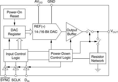
Simplified Schematic

3 Description
The DAC8311 (14-bit) and DAC8411 (16-bit) devices are low-power, single-channel, voltage output digital-to-analog converters (DAC). They provide excellent linearity and minimize undesired code-to-code transient voltages while offering an easy upgrade path within a pin-compatible family. All devices use a versatile, 3-wire serial interface that operates at clock rates of up to 50 MHz and is compatible with standard SPI™, QSPI™, Microwire, and digital signal processor (DSP) interfaces.
All devices use an external power supply as a reference voltage to set the output range. The devices incorporate a power-on reset (POR) circuit that ensures the DAC output powers up at 0 V and remains there until a valid write to the device occurs. The DAC8311 and DAC8411 contain a power-down feature, accessed over the serial interface, that reduces current consumption of the device to 0.1 μA at 2 V in power down mode. The low power consumption of these devices in normal operation makes it ideally suited for portable, battery-operated equipment. The power consumption is 0.55 mW at 5 V, reducing to 2.5 μW in power-down mode.
These devices are pin-compatible with the DAC5311, DAC6311, and DAC7311, offering an easy upgrade path from 8-, 10-, and 12-bit resolution to 14- and 16-bit. All devices are available in a small, 6-pin, SC70 package. This package offers a flexible, pin-compatible, and functionally-compatible drop-in solution within the family over an extended temperature range of –40°C to 125°C.
Device Information(1)
| PART NUMBER | PACKAGE | BODY SIZE (NOM) |
|---|---|---|
| DAC8311 DAC8411 |
SC70 (6) | 2.00 mm × 1.25 mm |
- For all available packages, see the orderable addendum at the end of the data sheet.