-
DRV2625 Ultra Low Power Closed-Loop LRA/ERM Haptic Driver with Built-In Library
- 1 Features
- 2 Applications
- 3 Description
- 4 Revision History
- 5 Pin Configuration and Functions
- 6 Specifications
- 7 Parameter Measurement Information
-
8 Detailed Description
- 8.1 Overview
- 8.2 Functional Block Diagram
- 8.3
Feature Description
- 8.3.1 Support for ERM and LRA Actuators
- 8.3.2 Smart-Loop Architecture
- 8.3.3 Open-Loop Operation
- 8.3.4 Flexible Front-End Interface
- 8.3.5 Noise Gate Control
- 8.3.6 Edge Rate Control
- 8.3.7 Constant Vibration Strength
- 8.3.8 Battery Voltage Reporting
- 8.3.9 Ultra Low-Power Shutdown
- 8.3.10 Automatic Go-To-Stand-by (Low Power)
- 8.3.11 I2C Watchdog Timer
- 8.3.12 Device Protection
- 8.3.13 POR
- 8.3.14 Silicon Revision Control
- 8.3.15 Support for LRA and ERM Actuators
- 8.3.16 Multi-Purpose Pin Functionality
- 8.3.17 Automatic Transition to Standby State
- 8.3.18 Automatic Brake into Standby
- 8.3.19 Battery Monitoring and Power Preservation
- 8.4 Device Functional Modes
- 8.5 Operation During Exceptional Conditions
- 8.6
Programming
- 8.6.1 Auto-Resonance Engine Programming for the LRA
- 8.6.2 Automatic-Level Calibration Programming
- 8.6.3 I2C Interface
- 8.6.4 Programming for Open-Loop Operation
- 8.6.5 Programming for Closed-Loop Operation
- 8.6.6 Diagnostics Routine
- 8.6.7 Calibration Routine
- 8.6.8 Waveform Playback Programming
- 8.6.9 Waveform Setup and Playback
- 8.7
Register Map
- 8.7.1 Address: 0x00
- 8.7.2 Address: 0x01
- 8.7.3 Address: 0x02
- 8.7.4 Address: 0x03
- 8.7.5 Address: 0x04
- 8.7.6 Address: 0x05
- 8.7.7 Address: 0x06
- 8.7.8 Address: 0x07
- 8.7.9 Address: 0x08
- 8.7.10 Address: 0x09
- 8.7.11 Address: 0x0A
- 8.7.12 Address: 0x0B
- 8.7.13 Address: 0x0C
- 8.7.14 Address: 0x0D
- 8.7.15 Address: 0x0E
- 8.7.16 Address: 0x0F
- 8.7.17 Address: 0x10
- 8.7.18 Address: 0x11
- 8.7.19 Address: 0x12
- 8.7.20 Address: 0x13
- 8.7.21 Address: 0x14
- 8.7.22 Address: 0x15
- 8.7.23 Address: 0x16
- 8.7.24 Address: 0x17
- 8.7.25 Address: 0x18
- 8.7.26 Address: 0x19
- 8.7.27 Address: 0x1A
- 8.7.28 Address: 0x1B
- 8.7.29 Address: 0x1C
- 8.7.30 Address: 0x1D
- 8.7.31 Address: 0x1F
- 8.7.32 Address: 0x20
- 8.7.33 Address: 0x21
- 8.7.34 Address: 0x22
- 8.7.35 Address: 0x23
- 8.7.36 Address: 0x24
- 8.7.37 Address: 0x25
- 8.7.38 Address: 0x26
- 8.7.39 Address: 0x27
- 8.7.40 Address: 0x28
- 8.7.41 Address: 0x29
- 8.7.42 Address: 0x2A
- 8.7.43 Address: 0x2C
- 8.7.44 Address: 0x2E
- 8.7.45 Address: 0x2F
- 8.7.46 Address: 0x30
- 9 Application and Implementation
- 10Power Supply Recommendations
- 11Layout
- 12Device and Documentation Support
- 13Mechanical, Packaging, and Orderable Information
- IMPORTANT NOTICE
Package Options
Refer to the PDF data sheet for device specific package drawings
Mechanical Data (Package|Pins)
- YFF|9
Thermal pad, mechanical data (Package|Pins)
Orderable Information
DRV2625 Ultra Low Power Closed-Loop LRA/ERM Haptic Driver with Built-In Library
1 Features
- Ultra Low-Power Shutdown Mode
- Low-Power Standby State
- Resistance-Based Actuator Diagnostics
- SimpleDrive One-Wire Vibration Scheme
- Automatic Resonance Tracking and Reporting
- Automatic Overdrive and Braking
- Automatic Level Calibration
- Drive Compensation Over Battery Discharge
- Configurable Battery Monitor with Power Preservation
- Off-Resonance Driving with Auto-Braking
- LRA Waveform Shape Selection
- Licensed Immersion TouchSense® 2200
- Built-In Library with Loopable Waveform Sequencer
- Real-Time Playback (RTP) Mode
- I2C-Controlled Digital Playback Engine
- Hardware and Software Trigger Option
- Automatic Transition to Standby with Auto-Brake
- Optional Interrupt Pin
- 1.8-V Compatible, VDD Tolerant Digital Interface (1)
2 Applications
- Mobile Phones and Tablets
- Fitness Bands and Wearable Devices
- Remote Controls, Mice, and Peripheral Devices
- Touch-Enabled Devices
- Human-Machine Interfaces
3 Description
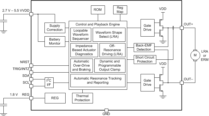
The DRV2625 device is a haptic driver that relies on a proprietary closed-loop architecture to deliver sharp, strong, and consistent haptic effects while optimizing power consumption.
The internal library and loopable waveform sequencer, together with the automatic overdrive and braking simplifies the process of generating crisp and optimum haptic effects, reducing the burden imposed into the processing unit.
The DRV2625 device features an automatic go-to-standby state and a battery preservation function to help reduce power consumption without user intervention. The NRST pin allows for a full shutdown state for additional power savings.
The waveform shape selection allows for sine-wave and square-wave drive to customize the haptic feel as well as the audible performance. Off-resonance driving with automatic braking simplifies the implementation of non-resonant haptic solutions.
Device Information(1)
| DEVICE NAME | PACKAGE | BODY SIZE (MAX) |
|---|---|---|
| DRV2625 | DSBGA (9) | 1.498 mm × 1.361 mm |
Simplified Schematic
4 Revision History
Changes from A Revision (December 2015) to B Revision
- Updated REV[3:0] from 2 to 3 Go
- Changed Default of 0x00 Register Go
- Changed Default of 0x07 Register Go
- Changed Bits 7 and 6 of 0x0D Register Go
- Changed the calculation value for the open loop LRA drive of register 0x2E from 'OL_LRA_PERIOD[9:0] × 24.39 µs' to 'OL_LRA_PERIOD[9:0] × 24.615 µs'Go
Changes from * Revision (December 2015) to A Revision
- Changed data sheet from Product Preview to Production DataGo
5 Pin Configuration and Functions
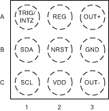
Pin Functions
| PIN | I/O | DESCRIPTION | |
|---|---|---|---|
| NAME | NO. | ||
| VDD | C2 | P | Supply input (2.7 V to 5.5 V). A 0.1-µF capacitor is required. |
| GND | B3 | P | Supply ground |
| REG | A2 | O | 1.8 V regulator output. A 0.1-µF capacitor is required |
| OUT- | C3 | O | Negative haptic driver differential output |
| OUT+ | A3 | O | Positive haptic driver differential output |
| SDA | B1 | I/O | I2C data |
| SCL | C1 | I | I2C clock |
| TRIG/INTZ | A1 | I/O |
Multi-mode pin. Selectable as input trigger (pulse), input enable, or output interrupt. This pin has an internal pull-down. If pin is not used, it should be connected to ground. |
| NRST | B2 | I | Device reset pin (shutdown mode). If pin is not used, it should be connected to VDD (no internal pull-up or pull-down). |
6 Specifications
6.1 Absolute Maximum Ratings
over operating free-air temperature range (unless otherwise noted) (1)| MIN | MAX | UNIT | ||
|---|---|---|---|---|
| Supply Voltage | VDD | –0.3 | 6 | V |
| Input voltage | NRST | –0.3 | 6 | V |
| SDA | –0.3 | 6 | V | |
| SCL | –0.3 | 6 | V | |
| TRIG/INTZ | –0.3 | 6 | V | |
| Operating free-air temperature range, TA | –40 | 85 | °C | |
| Operating junction temperature range, TJ | –40 | 150 | °C | |
| Storage temperature, Tstg | –65 | 150 | °C | |
6.2 ESD Ratings
| MIN | MAX | UNIT | |||
|---|---|---|---|---|---|
| V(ESD) | Electrostatic discharge | Human body model (HBM), per ANSI/ESDA/JEDEC JS-001, all pins(1) | –1500 | 1500 | V |
| Charged device model (CDM), per JEDEC specification JESD22-C101, all pins(2) | –500 | 500 | |||
6.3 Recommended Operating Conditions
over operating free-air temperature range (unless otherwise noted)| MIN | NOM | MAX | UNIT | ||
|---|---|---|---|---|---|
| VDD | Supply voltage | 2.7 | 5.5 | V | |
| RL | Load impedance | 8 | Ω | ||
| CL | Load capacitance | 100 | pF | ||
| ƒ(LRA) | LRA frequency | 45 | 300 | Hz | |
6.4 Thermal Information
| THERMAL METRIC(1) | DRV2625 | UNIT | |
|---|---|---|---|
| DSBGA | |||
| 9 PINS | |||
| RθJA | Junction-to-ambient thermal resistance | 107 | °C/W |
| RθJC(top) | Junction-to-case (top) thermal resistance | 0.9 | °C/W |
| RθJB | Junction-to-board thermal resistance | 18.1 | °C/W |
| ψJT | Junction-to-top characterization parameter | 3.8 | °C/W |
| ψJB | Junction-to-board characterization parameter | 18.1 | °C/W |
| RθJC(bot) | Junction-to-case (bottom) thermal resistance | — | °C/W |
6.5 Electrical Characteristics
TA = 25 °C, VDD = 3.6 V (unless otherwise noted)| PARAMETER | TEST CONDITIONS | MIN | TYP | MAX | UNIT | |
|---|---|---|---|---|---|---|
| V(REG) | Voltage at the REG pin | 1.84 | V | |||
| IIL | Digital low-level input current | NRST, TRIG/INTZ, SDA, SCL VDD = 5.5 V, VI = 0 V |
100 | nA | ||
| IIH | Digital high-level input current | SDA, SCL VDD = 5.5 V, VI = VDD |
0.1 | µA | ||
| NRST VDD = 5.5 V, VI = VDD |
1 | |||||
| TRIG/INTZ VDD = 5.5 V, VI = VDD |
2.7 | 3.5 | ||||
| VIL | Digital low-level input voltage | NRST, TRIG/INTZ, SDA, SCL | 0.4 | V | ||
| VIH | Digital high-level input voltage | NRST, TRIG/INTZ, SDA, SCL | 1.41 | V | ||
| VOL | Digital low-level output voltage | TRIG/INTZ, SDA 3-mA sink current |
0.4 | V | ||
| RDS(on) | Drain-source on-state resistance (LS + HS) | 0.75 | Ω | |||
| I(SD) | Shutdown current | V(NRST) = 0 V | 105 | 180 | nA | |
| I(STBY) | Standby current | V(NRST) = VDD
In stand-by mode |
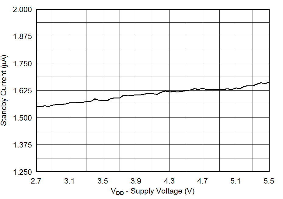
1.55 | 2 | µA | |
| I(Q) | Quiescent current | V(NRST) = VDD
In idle mode - no signal |
2.5 | mA | ||
| ZO(SD) | Output impedance in shutdown | OUT+ to GND, OUT– to GND | 15 | kΩ | ||
| ZO(STBY) | Output impedance in standby | OUT+ to GND, OUT– to GND | 15 | kΩ | ||
| ZLOAD(th) | Load impedance threshold for over-current detection | OUT+ to GND, OUT– to GND | 4 | Ω | ||
6.6 Timing Requirements
TA = 25 °C, VDD = 3.6 V (unless otherwise noted)| MIN | NOM | MAX | UNIT | ||
|---|---|---|---|---|---|
| ƒ(SCL) | Frequency at the SCL pin with no wait states | 400 | kHz | ||
| tw(H) | Pulse duration, SCL high | 0.6 | µs | ||
| tw(L) | Pulse duration, SCL low | 1.3 | µs | ||
| tsu(1) | Setup time, SDA to SCL | 100 | ns | ||
| th(1) | Hold time, SCL to SDA | 10 | ns | ||
| t(BUF) | Bus free time between stop and start condition | 1.3 | µs | ||
| tsu(2) | Setup time, SCL to start condition | 0.6 | µs | ||
| th(2) | Hold time, start condition to SCL | 0.6 | µs | ||
| tsu(3) | Setup time, SCL to stop condition | 0.6 | µs | ||
6.7 Switching Characteristics
TA = 25 °C, VDD = 3.6 V (unless otherwise noted)| PARAMETER | TEST CONDITIONS | MIN | TYP | MAX | UNIT | |
|---|---|---|---|---|---|---|
| t(on) | Device startup time | from shutdown standby | 1 | ms | ||
| t(start) | Waveform startup time | from trigger to output signal | 1 | ms | ||
| fO(PWM) | PWM output frequency (in OUT+ and OUT-) | 20.5 | kHz | |||
 Figure 1. SCL and SDA Timing
 Figure 2. Timing for Start and Stop Conditions
6.8 Typical Characteristics
| VDD = 3.6 V | |
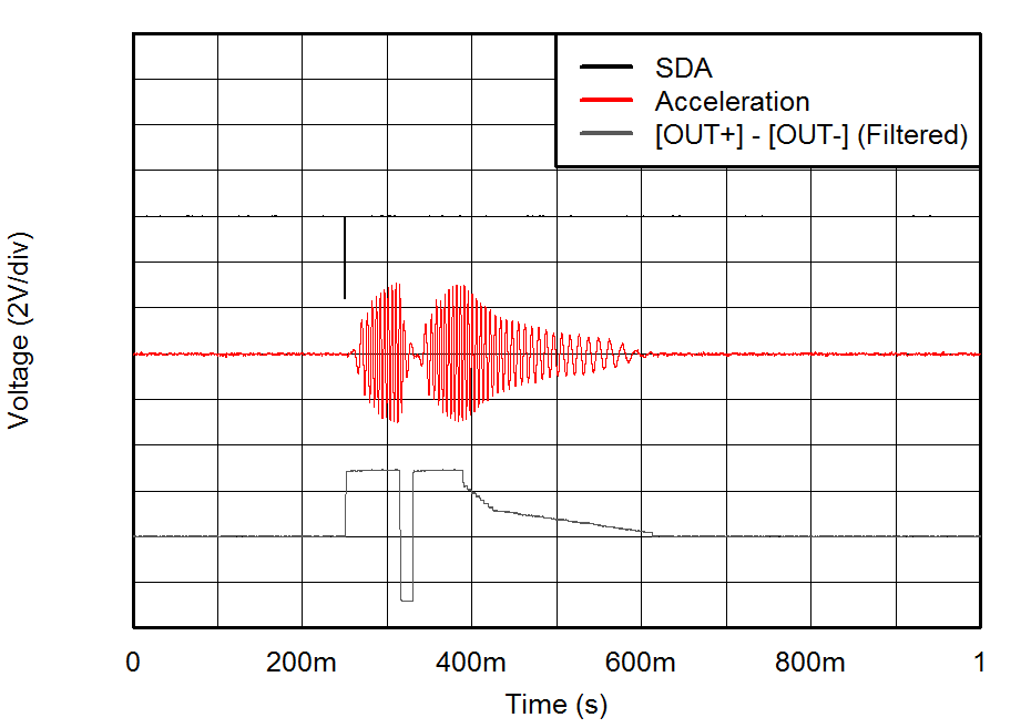
| VDD = 3.6 V | |
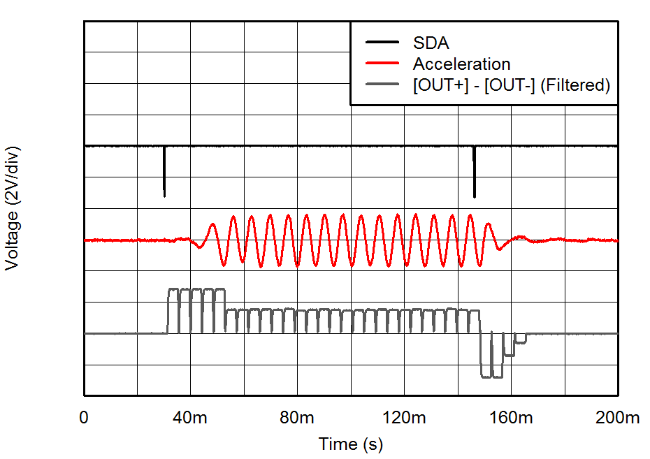
| VDD = 3.6 V | |

| VDD = 3.6 V | |
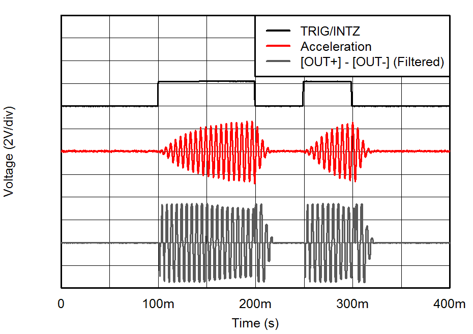
| VDD = 3.6 V | |
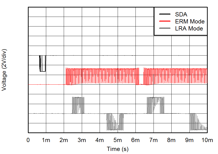
| VDD = 3.6 V | |
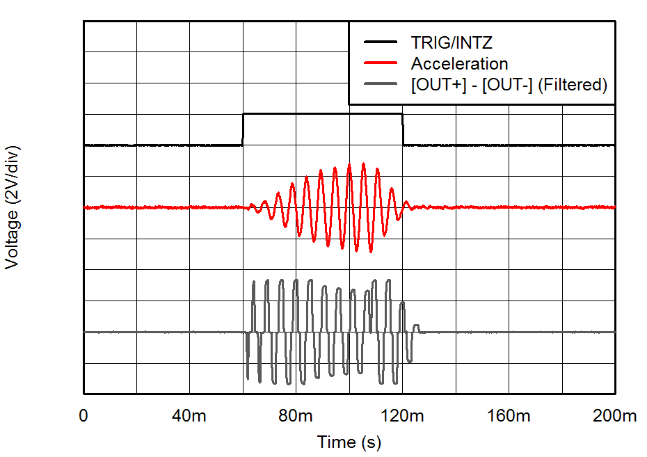
| VDD = 3.6 V | |
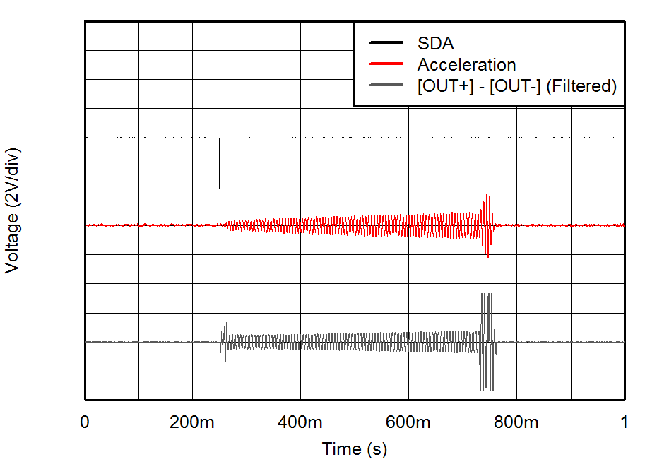
| VDD = 3.6 V | |
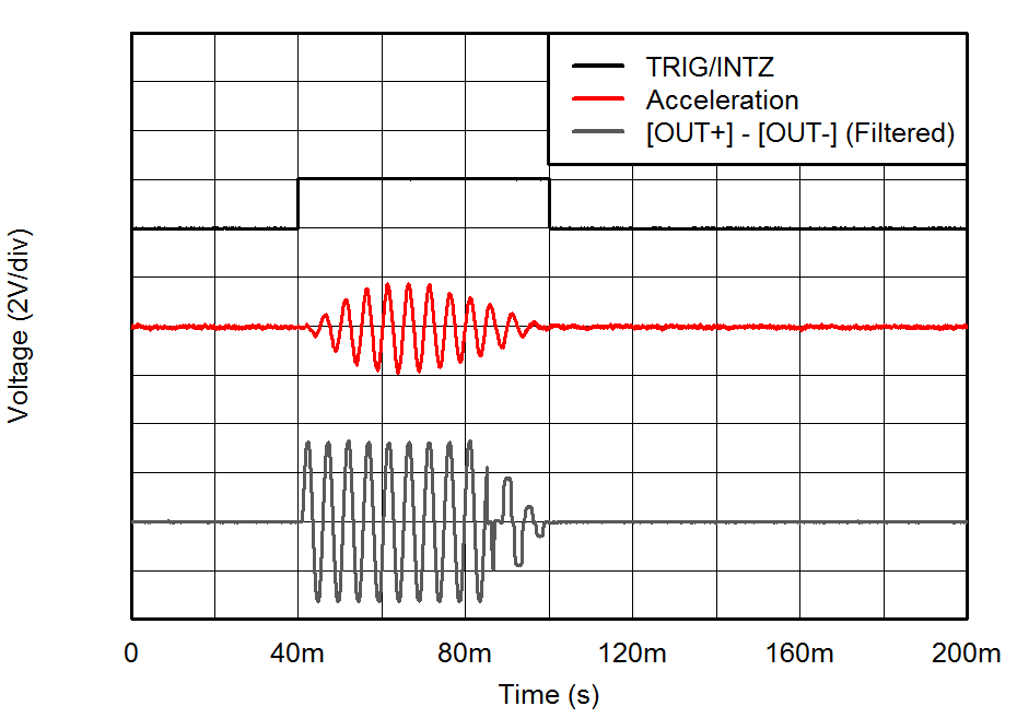
| VDD = 3.6 V | |
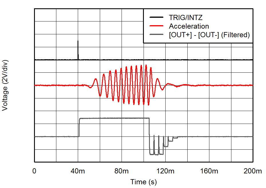
| VDD = 3.6 V | |
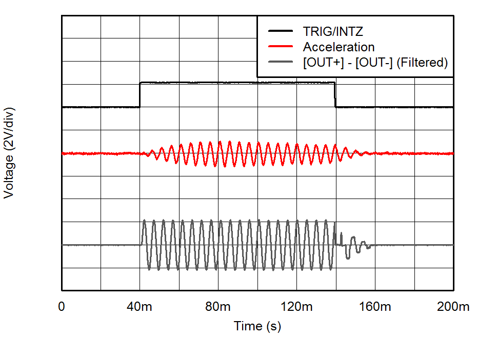
| VDD = 3.6 V | |