DRV8825 Stepper Motor Controller IC
1 Features
-
PWM Microstepping Stepper Motor Driver
- Built-In Microstepping Indexer
- Up to 1/32 Microstepping
- Multiple Decay Modes
- Mixed Decay
- Slow Decay
- Fast Decay
- 8.2-V to 45-V Operating Supply Voltage Range
- 2.5-A Maximum Drive Current at 24 V and
TA = 25°C - Simple STEP/DIR Interface
- Low Current Sleep Mode
- Built-In 3.3-V Reference Output
- Small Package and Footprint
- Protection Features
- Overcurrent Protection (OCP)
- Thermal Shutdown (TSD)
- VM Undervoltage Lockout (UVLO)
- Fault Condition Indication Pin (nFAULT)
2 Applications
- Automatic Teller Machines
- Money Handling Machines
- Video Security Cameras
- Printers
- Scanners
- Office Automation Machines
- Gaming Machines
- Factory Automation
- Robotics
3 Description
The DRV8825 provides an integrated motor driver solution for printers, scanners, and other automated equipment applications. The device has two H-bridge drivers and a microstepping indexer, and is intended to drive a bipolar stepper motor. The output driver block consists of N-channel power MOSFET’s configured as full H-bridges to drive the motor windings. The DRV8825 is capable of driving up to 2.5 A of current from each output (with proper heat sinking, at 24 V and 25°C).
A simple STEP/DIR interface allows easy interfacing to controller circuits. Mode pins allow for configuration of the motor in full-step up to 1/32-step modes. Decay mode is configurable so that slow decay, fast decay, or mixed decay can be used. A low-power sleep mode is provided which shuts down internal circuitry to achieve very low quiescent current draw. This sleep mode can be set using a dedicated nSLEEP pin.
Internal shutdown functions are provided for overcurrent, short circuit, under voltage lockout and over temperature. Fault conditions are indicated via the nFAULT pin.
Device Information(1)
| PART NUMBER | PACKAGE | BODY SIZE (NOM) |
|---|---|---|
| DRV8825 | HTSSOP (28) | 9.70 mm × 6.40 mm |
- For all available packages, see the orderable addendum at the end of the data sheet.
4 Simplified Schematic

Microstepping Current Waveform

5 Revision History
Changes from E Revision (August 2013) to F Revision
- Added new sections and reordered data sheet to fit new TI flowGo
- Updated pin descriptions Go
- Added power supply ramp rate and updated ISENSEx pin voltage in Absolute Maximum RatingsGo
- Updated VIL voltage minimum and typical in Electrical CharacteristicsGo
- Updated IIN and tDEG in Electrical Characteristics Go
6 Pin Configuration and Functions

Pin Functions
| PIN | I/O(1) | DESCRIPTION | EXTERNAL COMPONENTS OR CONNECTIONS |
|
|---|---|---|---|---|
| NAME | NO. | |||
| POWER AND GROUND | ||||
| CP1 | 1 | I/O | Charge pump flying capacitor | Connect a 0.01-μF 50-V capacitor between CP1 and CP2. |
| CP2 | 2 | I/O | Charge pump flying capacitor | |
| GND | 14, 28 | — | Device ground | |
| VCP | 3 | I/O | High-side gate drive voltage | Connect a 0.1-μF 16-V ceramic capacitor and a 1-MΩ resistor to VM. |
| VMA | 4 | — | Bridge A power supply | Connect to motor supply (8.2 to 45 V). Both pins must be connected to the same supply, bypassed with a 0.1-µF capacitor to GND, and connected to appropriate bulk capacitance. |
| VMB | 11 | — | Bridge B power supply | |
| V3P3OUT | 15 | O | 3.3-V regulator output | Bypass to GND with a 0.47-μF 6.3-V ceramic capacitor. Can be used to supply VREF. |
| CONTROL | ||||
| AVREF | 12 | I | Bridge A current set reference input | Reference voltage for winding current set. Normally AVREF and BVREF are connected to the same voltage. Can be connected to V3P3OUT. |
| BVREF | 13 | I | Bridge B current set reference input | |
| DECAY | 19 | I | Decay mode | Low = slow decay, open = mixed decay, high = fast decay. Internal pulldown and pullup. |
| DIR | 20 | I | Direction input | Level sets the direction of stepping. Internal pulldown. |
| MODE0 | 24 | I | Microstep mode 0 | MODE0 through MODE2 set the step mode - full, 1/2, 1/4, 1/8/ 1/16, or 1/32 step. Internal pulldown. |
| MODE1 | 25 | I | Microstep mode 1 | |
| MODE2 | 26 | I | Microstep mode 2 | |
| NC | 23 | — | No connect | Leave this pin unconnected. |
| nENBL | 21 | I | Enable input | Logic high to disable device outputs and indexer operation, logic low to enable. Internal pulldown. |
| nRESET | 16 | I | Reset input | Active-low reset input initializes the indexer logic and disables the H-bridge outputs. Internal pulldown. |
| nSLEEP | 17 | I | Sleep mode input | Logic high to enable device, logic low to enter low-power sleep mode. Internal pulldown. |
| STEP | 22 | I | Step input | Rising edge causes the indexer to move one step. Internal pulldown. |
| STATUS | ||||
| nFAULT | 18 | OD | Fault | Logic low when in fault condition (overtemp, overcurrent) |
| nHOME | 27 | OD | Home position | Logic low when at home state of step table |
| OUTPUT | ||||
| AOUT1 | 5 | O | Bridge A output 1 | Connect to bipolar stepper motor winding A. Positive current is AOUT1 → AOUT2 |
| AOUT2 | 7 | O | Bridge A output 2 | |
| BOUT1 | 10 | O | Bridge B output 1 | Connect to bipolar stepper motor winding B. Positive current is BOUT1 → BOUT2 |
| BOUT2 | 8 | O | Bridge B output 2 | |
| ISENA | 6 | I/O | Bridge A ground / Isense | Connect to current sense resistor for bridge A. |
| ISENB | 9 | I/O | Bridge B ground / Isense | Connect to current sense resistor for bridge B. |
7 Specifications
7.1 Absolute Maximum Ratings(1)(2)
| MIN | MAX | UNIT | |||
|---|---|---|---|---|---|
| V(VMx) | Power supply voltage | –0.3 | 47 | V | |
| Power supply ramp rate | 1 | V/µs | |||
| Digital pin voltage | –0.5 | 7 | V | ||
| V(xVREF) | Input voltage | –0.3 | 4 | V | |
| ISENSEx pin voltage(4) | –0.8 | 0.8 | V | ||
| Peak motor drive output current, t < 1 μs | Internally limited | A | |||
| Continuous motor drive output current(3) | 0 | 2.5 | A | ||
| Continuous total power dissipation | See Thermal Information | ||||
| TJ | Operating junction temperature range | –40 | 150 | °C | |
7.2 Handling Ratings
| MIN | MAX | UNIT | |||
|---|---|---|---|---|---|
| Tstg | Storage temperature range | –60 | 150 | °C | |
| V(ESD) | Electrostatic discharge | Human body model (HBM), per ANSI/ESDA/JEDEC JS-001, all pins(1) | –2000 | 2000 | V |
| Charged device model (CDM), per JEDEC specification JESD22-C101, all pins(2) | –500 | 500 | |||
7.3 Recommended Operating Conditions
| MIN | NOM | MAX | UNIT | ||
|---|---|---|---|---|---|
| V(VMx) | Motor power supply voltage range(1) | 8.2 | 45 | V | |
| V(VREF) | VREF input voltage(2) | 1 | 3.5 | V | |
| IV3P3 | V3P3OUT load current | 0 | 1 | mA | |
7.4 Thermal Information
| THERMAL METRIC(1) | DRV8825 | UNIT | |
|---|---|---|---|
| PWP | |||
| 28 PINS | |||
| RθJA | Junction-to-ambient thermal resistance(2) | 31.6 | °C/W |
| RθJC(top) | Junction-to-case (top) thermal resistance(3) | 15.9 | |
| RθJB | Junction-to-board thermal resistance(4) | 5.6 | |
| ψJT | Junction-to-top characterization parameter(5) | 0.2 | |
| ψJB | Junction-to-board characterization parameter(6) | 5.5 | |
| RθJC(bot) | Junction-to-case (bottom) thermal resistance(7) | 1.4 | |
7.5 Electrical Characteristics
over operating free-air temperature range of –40°C to 85°C (unless otherwise noted)7.6 Timing Requirements
| MIN | MAX | UNIT | |||
|---|---|---|---|---|---|
| 1 | ƒSTEP | Step frequency | 250 | kHz | |
| 2 | tWH(STEP) | Pulse duration, STEP high | 1.9 | μs | |
| 3 | tWL(STEP) | Pulse duration, STEP low | 1.9 | μs | |
| 4 | tSU(STEP) | Setup time, command before STEP rising | 650 | ns | |
| 5 | tH(STEP) | Hold time, command after STEP rising | 650 | ns | |
| 6 | tENBL | Enable time, nENBL active to STEP | 650 | ns | |
| 7 | tWAKE | Wakeup time, nSLEEP inactive high to STEP input accepted | 1.7 | ms | |
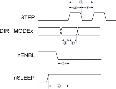 Figure 1. Timing Diagram
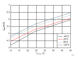
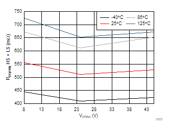
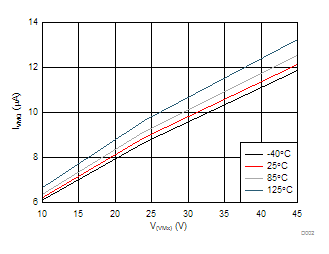
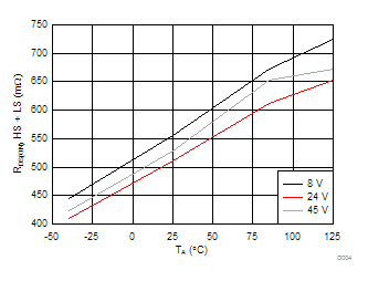
7.7 Typical Characteristics