DS100DF410 Low Power 10GbE Quad Channel Retimer
1 Features
- Each Channel Independently Locks to 10.3125 Gbps
- Lock Operation (typically under 15 ms)
- Low Latency (~300 ps)
- Adaptive Equalization up to 34 dB Boost at 5 GHz
- Adjustable Transmit VOD: 600 to 1300 mVp-p
- Adjustable Transmit De-emphasis to –12 dB
- Typical Power Dissipation (EQ+DFE+CDR+DE): 180 mW/channel
- Programmable Output Polarity Inversion
- Input Signal Detection, CDR Lock Detection/Indicator
- On-chip Eye Monitor (EOM), PRBS Generator
- Single 2.5 V ±5% Power Supply
- SMBus/EEPROM Configuration Modes
- Operating Temperature Range of –40°C to 85°C
- WQFN 48-Pin, 7 mm x 7 mm Package
- Easy Pin Compatible Upgrade Between Repeater and Retimers
- DS100RT410 (EQ+CDR+DE): 10.3125 Gbps
- DS100DF410 (EQ+DFE+CDR+DE): 10.3125 Gbps
- DS110RT410 (EQ+CDR+DE): 8.5–11.3 Gbps
- DS110DF410 (EQ+DFE+CDR+DE): 8.5–11.3 Gbps
- DS125RT410 (EQ+CDR+DE): 9.8–12.5 Gbps
- DS125DF410 (EQ+DFE+CDR+DE): 9.8–12.5 Gbps
- DS100BR410 (EQ+DE): Up to 10.3125 Gbps
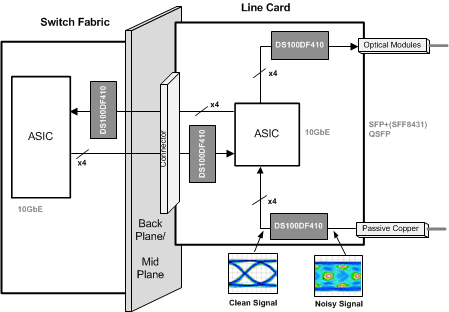
2 Applications
- Front Port SFF 8431 (SFP+) Optical and Direct Attach Copper
- Backplane Reach Extension, Data Retimer
- Ethernet: 10GbE, 1GbE
For other data rates and data transmission protocols, other pin-compatible devices in the retimer family can be used.
3 Description
The DS100DF410 is four channel retimers with integrated signal conditioning. Each channel can independently lock to 10.3125 Gbps data rate to support 10GbE. The device includes a fully adaptive Continuous-Time Linear Equalizer (CTLE), Clock and Data Recovery (CDR) and transmit De-Emphasis (DE) driver. The DS100DF410 also includes a self calibrating 5-tap Decision Feedback Equalizer (DFE) to enable data transmission over long, lossy and crosstalk-impaired highspeed serial links to achieve BER < 1×10-15.
The programmable settings can be applied easily using the SMBus (I2C) interface, or they can be loaded via an external EEPROM. An on-chip eye monitor and a PRBS generator allow real-time measurement of high-speed serial data for system bring-up or field tuning. Flow-through pinout and single power supply make the DS100DF410 easy to use.
Device Information(1)
| PART NUMBER | PACKAGE | BODY SIZE (NOM) |
|---|---|---|
| DS100DF410SQ | WQFN (48) | 7.00 mm × 7.00 mm |
- For all available packages, see the orderable addendum at the end of the data sheet.
Typical Application Diagram
4 Revision History
Changes from A Revision (February 2013) to B Revision
- Changed ESD Ratings table, Feature Description section, Device Functional Modes, Application and Implementation section, Power Supply Recommendations section, Layout section, Device and Documentation Support section, and Mechanical, Packaging, and Orderable Information sectionGo
5 Pin Configuration and Functions

Pin Functions
| PIN | TYPE(1) | DESCRIPTION | |
|---|---|---|---|
| NAME | NUMBER | ||
| HIGH-SPEED DIFFERENTIAL I/O | |||
| RXP0 RXN0 |
1 2 |
I, CML | Inverting and non-inverting CML-compatible differential inputs to the equalizer. Nominal differential input impedance = 100Ω. Must be AC coupled. |
| RXP1 RXN1 |
4 5 |
I, CML | Inverting and non-inverting CML-compatible differential inputs to the equalizer. Nominal differential input impedance = 100Ω. Must be AC coupled. |
| RXP2 RXN2 |
8 9 |
I, CML | Inverting and non-inverting CML-compatible differential inputs to the equalizer. Nominal differential input impedance = 100Ω. Must be AC coupled. |
| RXP3 RXN3 |
11 12 |
I, CML | Inverting and non-inverting CML-compatible differential inputs to the equalizer. Nominal differential input impedance = 100Ω. Must be AC coupled. |
| TXP0 TXN0 |
36 35 |
O, CML | Inverting and non-inverting CML-compatible differential outputs from the driver. Nominal differential output impedance = 100Ω. Must be AC coupled. |
| TXP1 TXN1 |
33 32 |
O, CML | Inverting and non-inverting CML-compatible differential outputs from the driver. Nominal differential output impedance = 100Ω. Must be AC coupled. |
| TXP2 TXN2 |
29 28 |
O, CML | Inverting and non-inverting CML-compatible differential outputs from the driver. Nominal differential output impedance = 100Ω. Must be AC coupled. |
| TXP3 TXN3 |
26 25 |
O, CML | Inverting and non-inverting CML-compatible differential outputs from the driver. Nominal differential output impedance = 100Ω. Must be AC coupled. |
| LOOP FILTER CONNECTION PINS | |||
| LPF_CP_0 LPF_REF_0 |
47 48 |
I/O, analog | Loop filter connection Place a 22 nF ± 10% Capacitor between LPF_CP_0 and LPF_REF_0 |
| LPF_CP_1 LPF_REF_1 |
38 37 |
I/O, analog | Loop filter connection Place a 22 nF ± 10% Capacitor between LPF_CP_1 and LPF_REF_1 |
| LPF_CP_2 LPF_REF_2 |
23 24 |
I/O, analog | Loop filter connection Place a 22 nF ± 10% Capacitor between LPF_CP_2 and LPF_REF_2 |
| LPF_CP_3 LPF_REF_3 |
14 13 |
I/O, analog | Loop filter connection Place a 22 nF ± 10% Capacitor between LPF_CP_3 and LPF_REF_3 |
| REFERENCE CLOCK I/O | |||
| REFCLK_IN | 19 | I, 2.5V analog | Input is 2.5 V, 25 MHz ± 100 ppm reference clock from external oscillator No stringent phase noise requirement |
| REFCLK_OUT | 42 | O, 2.5V analog | Output is 2.5 V, buffered replica of reference clock input for connecting multiple DS100DF410s on a board |
| LOCK INDICATOR PINS | |||
| LOCK_0 LOCK_1 LOCK_2 LOCK_3 |
45 40 21 16 |
O, 2.5V LVCMOS | Output is 2.5 V, the pin is high when CDR lock is attained on the corresponding channel Note that these pins are shared with SMBus address strap input functions read at startup. |
| SMBus MASTER MODE PINS | |||
| ALL_DONE | 41 | O, 2.5V LVCMOS | Output is 2.5 V, the pin goes low to indicate that the SMBus master EEPROM read has been completed. |
| READ_EN | 44 | I, 2.5V LVCMOS | Input is 2.5 V, a transition from high to low starts the load from the external EEPROM. The READ_EN pin must be tied low when in SMBus slave mode |
| INTERRUPT OUTPUT | |||
| INT | 43 | O, 3.3V LVCMOS, Open Drain | Used to signal horizontal or vertical eye opening out of tolerance, loss of signal detect, or CDR unlock External 2KΩ to 5KΩ pull-up resistor is required. Pin is 3.3 V LVCMOS tolerant. |
| SERIAL MANAGEMENT BUS (SMBus) INTERFACE | |||
| EN_SMB | 20 | I, 2.5V analog | Input is 2.5 V, selects SMBus master mode or SMBus slave mode EN_SMB = High for slave mode EN_SMB = Float for master mode Tie READ_EN pin low for SMBus slave mode. See Table 1 |
| SDA | 18 | I/O, 3.3V LVCMOS, Open Drain | Data Input / Open Drain Output External 2KΩ to 5KΩ pull-up resistor is required. Pin is 3.3 V LVCMOS tolerant. |
| SDC | 17 | I/O, 3.3V LVCMOS, Open Drain | Clock Input / Open Drain Clock Output External 2KΩ to 5KΩ pull-up resistor is required. Pin is 3.3 V LVCMOS tolerant. |
| ADDR_0 ADDR_1 ADDR_2 ADDR_3 |
45 40 21 16 |
I, 2.5V LVCMOS | Input is 2.5 V, the ADDR_[3:0] pins set the SMBus address for the retimer. These pins are strap inputs. Their state is read on power-up to set the SMBus address in SMBus control mode. High = 1KΩ to VDD, Low = 1KΩ to GND Note that these pins are shared with the lock indicator functions. See Table 2 |
| POWER | |||
| VDD | 3, 6, 7, 10, 15, 46 |
Power | VDD = 2.5 V ± 5% |
| GND | 22, 27, 30, 31, 34, 39 |
Power | Ground reference. |
| DAP | PAD | Power | Ground reference. The exposed pad at the center of the package must be connected to ground plane of the board with at least 4 vias to lower the ground impedance and improve the thermal performance of the package. |
Only SMBus pins SDA and SDC and INT pin are 3.3 V tolerant. These three pins are open-drain and require external pull-up resistors.
6 Specifications
6.1 Absolute Maximum Ratings (1)
over operating free-air temperature range (unless otherwise noted)6.2 ESD Ratings
| VALUE | UNIT | |||
|---|---|---|---|---|
| V(ESD) | ESD Rating | Human Body Model (HBM), per ANSI/ESDA/JEDEC JS-001, all pins(1) | ±6000 | V |
| Machine Model (MM), STD - JESD22-A115-A(3) | ±250 | |||
| Charged Device Model (CDM), per JEDEC specification JESD22-C101, all pins(2) | ±1250 | |||
6.3 Recommended Operating Conditions
over operating free-air temperature range (unless otherwise noted)| MIN | NOM | MAX | UNIT | |
|---|---|---|---|---|
| Supply Voltage (VDD to GND) | 2.375 | 2.5 | 2.625 | V |
| Ambient Temperature | -40 | 25 | +85 | °C |
6.4 Thermal Information(2)
| THERMAL METRIC(1) | DS100DF410 | UNIT | |
|---|---|---|---|
| WQFN | |||
| 48 PINS | |||
| RθJA | Junction-to-ambient thermal resistance | 26.1 | °C/W |
6.5 Electrical Characteristics
Over recommended operating supply and temperature ranges with default register settings unless otherwise specified. (1)| PARAMETER | TEST CONDITIONS | MIN | TYP | MAX | UNIT | |
|---|---|---|---|---|---|---|
| POWER | ||||||
| PD | Power supply consumption | Average Power Consumption(2) | 720 | mW | ||
| Max Transient Power Supply Current (3) | 500 | 610 | mA | |||
| NTPS | Supply noise tolerance (4) | 50 Hz to 100 Hz | 100 | mVP-P | ||
| 100 Hz to 10 MHz | 40 | mVP-P | ||||
| 10 MHz to 5.0 GHz | 10 | mVP-P | ||||
| 2.5V LVCMOS DC SPECIFICATIONS | ||||||
| VIH | High level input voltage | 1.75 | VDD | V | ||
| High level (ADDR[3:0] pins) | 2.28 | VDD | V | |||
| VIL | Low level input voltage | GND | 0.7 | V | ||
| Low level input voltage (ADDR[3:0] pins) | GND | 0.335 | V | |||
| VOH | High level output voltage | IOH = -3mA | 2.0 | V | ||
| VOL | Low level output voltage | IOL = 3mA | 0.4 | V | ||
| IIN | Input leakage current | VIN = VDD | 10 | μA | ||
| VIN = GND | –10 | μA | ||||
| IIH | Input high current (EN_SMB pin) | VIN = VDD | 55 | μA | ||
| IIL | Input low current (EN_SMB pin) | VIN = GND | –110 | μA | ||
| 3.3 V LVCMOS DC SPECIFICATIONS (SDA, SDC, INT) | ||||||
| VIH | High level input voltage | VDD = 2.5 V | 1.75 | 3.6 | V | |
| VIL | Low level input voltage | VDD = 2.5 V | GND | 0.7 | V | |
| VOL | Low level output voltage | IPULLUP = 3mA | 0.4 | V | ||
| IIH | Input high current | VIN = 3.6 V, VDD = 2.5 V | 20 | 40 | μA | |
| IIL | Input low current | VIN = GND, VDD = 2.5 V | –10 | 10 | μA | |
| fSDC | SMBus clock rate | Slave Mode | 10 | 400 | kHz | |
| Master Mode(5) | 400 | kHz | ||||
| DATA BIT RATES | ||||||
| RB | Bit rate range | 10.3125 Gbps Ethernet | 10.1 | 10.6 | Gbps | |
| 1.25 Gbps Ethernet | 1.2 | 1.3 | Gbps | |||
| SIGNAL DETECT | ||||||
| SDH | Signal detect ON threshold level | Default differential input signal level to assert signal detect, 10.3125 Gbps, PRBS-31 |
70 | mVp-p | ||
| SDL | Signal detect OFF threshold level | Default differential input signal level to de-assert signal detect, 10.3125 Gbps, PRBS-31 |
10 | mVp-p | ||
| RECEIVER INPUTS (RXPn, RXNn) | ||||||
| VTX2, min | Minimum source transmit launch signal level (IN, diff) | See (5) | 600 | mVP-P | ||
| VTX2, max | 1000 | mVP-P | ||||
| VTX1, max | See (6) | 1200 | mVP-P | |||
| VTX0, max | See (7) | 1600 | mVP-P | |||
| LRI | Maximum differential input return loss - |SDD11| | 100 MHz – 6 GHz(8) | -15 | dB | ||
| ZD | Differential input impedance | 100 MHz – 6 GHz | 100 | Ω | ||
| ZS | Single-ended input impedance | 100 MHz – 6 GHz | 50 | Ω | ||
| DRIVER OUTPUTS (TXPn, TXNn) | ||||||
| VOD0 | Differential output voltage | Differential measurement with OUT+ and OUT- terminated by 50Ω to GND, AC-Coupled, SMBus register VOD control (Register 0x2d bits 2:0) set to 0, minimum VOD De-emphasis control set to minimum (0 dB) |
400 | 675 | mVP-P | |
| VOD7 | Differential output voltage | Differential measurement with OUT+ and OUT- terminated by 50Ω to GND, AC-Coupled SMBus register VOD control (Register 0x2d bits 2:0) set to 7, maximum VOD De-emphasis control set to minimum (0 dB) |
1000 | mVP-P | ||
| VOD_DE | De-emphasis level (10) | Differential measurement with OUT+ and OUT- terminated by 50Ω to GND, AC-Coupled Set by SMBus register control to maximum de-emphasis setting Relative to the nominal 0 dB de-emphasis level set at the minimum de-emphasis setting |
-12 | dB | ||
| tR, tF | Transition time (rise and fall times)(10)(11) | Transition time control = Full Slew Rate | 39 | ps | ||
| Transition time control = Limited Slew Rate | 50 | ps | ||||
| LRO | Maximum differential output return loss - |SDD22| | 100 MHz – 6 GHz (8) | –15 | dB | ||
| tDP | Propagation delay | Retimed data(9) | 300 | ps | ||
| TDE | De-emphasis pulse duration(12) | Measured at VOD = 1000 mVP-P, de-emphasis setting = -12 dB | 75 | ps | ||
| TJ | Output total jitter | Measured at BER = 10-12(13) | 10 | ps | ||
| TSKEW | Intra pair skew | Difference in 50% crossing between TXPn and TXNn for any output | 3 | ps | ||
| Channel-to-channel skew | 7 | ps | ||||
| CLOCK AND DATA RECOVERY | ||||||
| BWPLL | PLL Bandwidth, -3 dB | Measured at 10.3125 Gbps | 5 | MHz | ||
| JTOL | Input sinusoidal jitter tolerance 10 kHz to 250 MHz sinusoidal jitter frequency |
Measured at BER = 10-15 | 0.6 | UI | ||
| JTRANS | Jitter transfer sinusoidal jitter at 10 MHz jitter frequency | Measured at BER = 10-15 | -6 | dB | ||
| TLOCK | CDR Lock Time | Measured at 10.3125 Gbps | 15 | ms | ||
| RECOMMENDED REFERENCE CLOCK SPECS | ||||||
| REFf | Input reference clock frequency | 24.9975 | 25 | 25.0025 | MHz | |
| REFCLK_INPW | Minimum REFCLK_IN Pulse Width | At REFCLK_IN pin | 4 | ns | ||
| REFCLK_ OUTDCD |
REFCLK_OUT duty cycle distortion | CL = 5 pF | 0.55 | ns | ||
| REFVIH | Reference clock input min high threshold | 1.75 | V | |||
| REFVIL | Reference clock input max low threshold | 0.7 | V | |||

