SNLS374D May 1998 – January 2015 DS8921
PRODUCTION DATA.
- 1 Features
- 2 Applications
- 3 Description
- 4 Revision History
- 5 Pin Configuration and Functions
-
6 Specifications
- 6.1 Absolute Maximum Ratings
- 6.2 ESD Ratings
- 6.3 Recommended Operating Conditions
- 6.4 Electrical Characteristics
- 6.5 Receiver Switching Characteristics
- 6.6 Driver Switching Characteristics: Single-Ended Characteristics
- 6.7 Driver Switching Characteristics: Differential Characteristics
- 6.8 Typical Characteristics
- 7 Parameter Measurement Information
- 8 Detailed Description
- 9 Application and Implementation
- 10Power Supply Recommendations
- 11Layout
- 12Device and Documentation Support
- 13Mechanical, Packaging, and Orderable Information
Package Options
Mechanical Data (Package|Pins)
- D|8
Thermal pad, mechanical data (Package|Pins)
Orderable Information
1 Features
- 12-ns Typical Propagation Delay
- Output Skew: 0.5 ns Typical
- Meets the Requirements of EIA Standard RS-422
- Complementary Driver Outputs
- High Differential or Common-Mode Input Voltage Ranges of ±7 V
- ±0.2 V Receiver Sensitivity Over the Input Voltage Range
- Receiver Input Hysteresis: 70 mV Typical
- DS8921AT Industrial Temperature Operation: (−40°C to +85°C)
2 Applications
- Differential Line Driver and Receiver for:
- ST506 Disk Drive Standard
- ST412 Disk Drive Standard
- ESDI Disk Drive Standard
- RS-422 Interface
3 Description
The DS8921, DS8921A, and DS8921AT devices are differential line driver and receiver pairs designed specifically for applications meeting the ST506, ST412, and ESDI disk drive standards. In addition, these devices meet the requirements of the EIA standard RS-422.
The DS8921x receivers offer an input sensitivity of 200 mV over a ±7 V common mode operating range. Hysteresis is incorporated (typically 70 mV) to improve noise margin for slowly changing input waveforms.
The DS8921x drivers are designed to provide unipolar differential drive to twisted-pair or parallel wire transmission lines. Complementary outputs are logically ANDed and provide an output skew of 0.5 ns (typical) with propagation delays of 12 ns.
The DS8921x devices are designed to be compatible with TTL and CMOS.
Device Information(1)
| PART NUMBER | PACKAGE | BODY SIZE (NOM) |
|---|---|---|
| DS8921 DS8921A DS8921AT |
SOIC (8) | 4.90 mm x 3.91 mm |
| PDIP (8) | 9.81 mm x 6.35 mm |
- For all available packages, see the orderable addendum at the end of the data sheet.
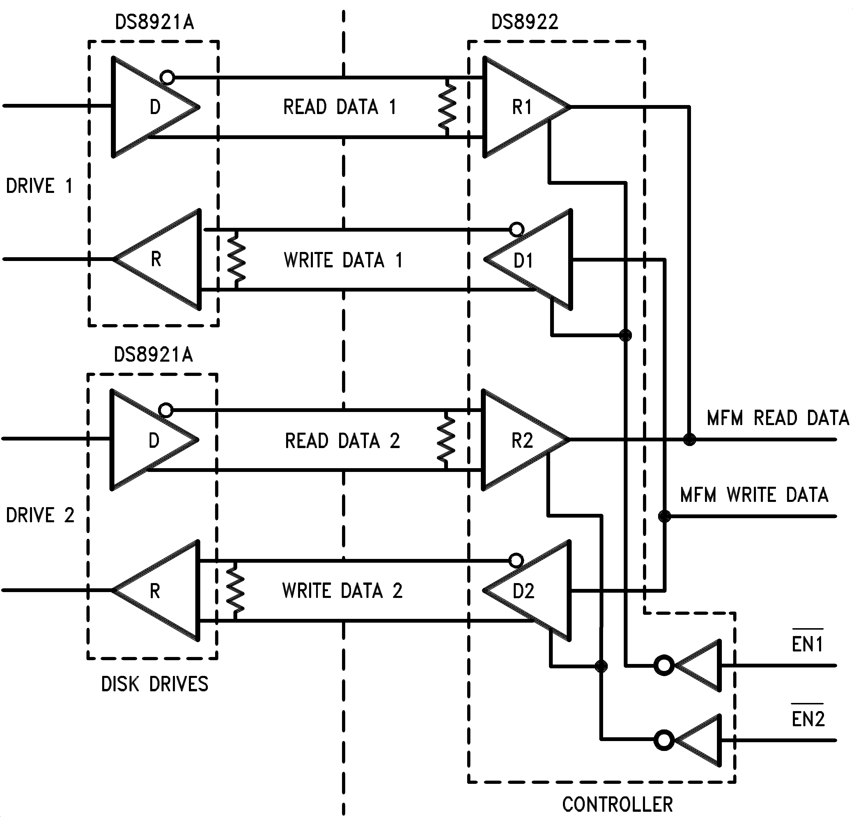
Typical Application Block Diagram

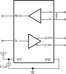
Simplified Functional Block Diagram
