SNLS512 April 2016 DS90UB924-Q1
PRODUCTION DATA.
- 1 Features
- 2 Applications
- 3 Description
- 4 Revision History
- 5 Pin Configuration and Functions
-
6 Specifications
- 6.1 Absolute Maximum Ratings
- 6.2 ESD Ratings
- 6.3 Recommended Operating Conditions
- 6.4 Thermal Information
- 6.5 DC Electrical Characteristics
- 6.6 AC Electrical Characteristics
- 6.7 DC and AC Serial Control Bus Characteristics
- 6.8 Timing Requirements for the Serial Control Bus
- 6.9 Timing Requirements
- 6.10 Typical Characteristics
-
7 Detailed Description
- 7.1 Overview
- 7.2 Functional Block Diagram
- 7.3
Feature Description
- 7.3.1 High-Speed Forward Channel Data Transfer
- 7.3.2 Low-Speed Back Channel Data Transfer
- 7.3.3 Backward Compatible Mode
- 7.3.4 Input Equalization
- 7.3.5 Common Mode Filter Pin (CMF)
- 7.3.6 Power Down (PDB)
- 7.3.7 Video Control Signals
- 7.3.8 EMI Reduction Features
- 7.3.9 Built In Self Test (BIST)
- 7.3.10 Internal Pattern Generation
- 7.3.11 Serial Link Fault Detect
- 7.3.12 Oscillator Output
- 7.3.13 Interrupt Pin (INTB / INTB_IN)
- 7.3.14 General-Purpose I/O
- 7.3.15 I2S Audio Interface
- 7.3.16 AV Mute Prevention
- 7.3.17 OEN Toggling Limitation
- 7.4 Device Functional Modes
- 7.5 Programming
- 7.6 Register Maps
- 8 Application and Implementation
- 9 Power Supply Recommendations
- 10Layout
- 11Device and Documentation Support
- 12Mechanical, Packaging, and Orderable Information
Package Options
Mechanical Data (Package|Pins)
- RHS|48
Thermal pad, mechanical data (Package|Pins)
- RHS|48
Orderable Information
1 Features
- Qualified for Automotive Applications AEC-Q100
- Device Temperature Grade 2: –40°C to +105°C Ambient Operating Temperature Range
- Device HBM ESD Classification Level ±8 kV
- Device CDM ESD Classification Level C6
- 5-MHz to 96-MHz Pixel Clock Support
- Bidirectional Control Channel Interface with I2C-Compatible Serial Control Bus
- Low EMI OpenLDI Video Output
- Supports High Definition (720p) Digital Video
- RGB888 + VS, HS, DE and I2S Audio Supported
- Up to 4 I2S Digital Audio Outputs for Surround Sound Applications
- 4 Bidirectional GPIO Channels With 2 Dedicated Pins
- Single 3.3-V Supply With 1.8-V or 3.3-V Compatible LVCMOS I/O Interface
- DC-Balanced and Scrambled Data with Embedded Clock
- Adaptive Cable Equalization
- Internal Pattern Generation
- Backward Compatible Modes
2 Applications
- Automotive Touch Screen Display
- Automotive Display for Navigation
- Automotive Instrument Cluster
3 Description
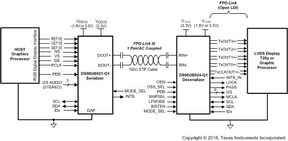
The DS90UB924-Q1 deserializer, in conjunction with a DS90UB921-Q1, DS90UB925Q-Q1, DS90UB927Q-Q1, DS90UB929-Q1, DS90UB949-Q1, or DS90UB947-Q1 serializer, provides a solution for distribution of digital video and audio within automotive infotainment systems. The device converts a high-speed serialized interface with an embedded clock, delivered over a single signal pair (FPD-Link III), to four LVDS data/control streams, one LVDS clock pair (OpenLDI), and I2S audio data. The serial bus scheme, FPD-Link III, supports high-speed forward channel data transmission and low-speed full duplex back channel communication over a single differential link. Consolidation of audio, video data and control over a single differential pair reduces the interconnect size and weight, while also eliminating skew issues and simplifying system design.
Adaptive input equalization of the serial input stream provides compensation for transmission medium losses and deterministic jitter. EMI is minimized by the use of low voltage differential signaling.
Device Information (1)
| PART NUMBER | PACKAGE | BODY SIZE (NOM) |
|---|---|---|
| DS90UB924-Q1 | WQFN (48) | 7.00 mm x 7.00 mm |
- For all available packages, see the orderable addendum at the end of the data sheet.
