INA12x-HT Precision, Low-Power Instrumentation Amplifiers
1 Features
- Low Offset Voltage: 25 uV Typical
- Low Input Bias Current: 50 nA Typical (1)
- High CMR: 95 dB Typical(1)
- Inputs Protected to ±40 V
- Wide Supply Range: ±2.25 V to ±18 V
- Low Quiescent Current: 2 mA Typical(1)
2 Applications
- Bridge Amplifiers
- Thermocouple Amplifiers
- RTD Sensor Amplifiers
- Medical Instrumentation
- Data Acquisition
- Supports Extreme Temperature Applications:
- Controlled Baseline
- One Assembly/Test Site
- One Fabrication Site
- Available in Extreme Temperature Ranges
(–55°C to 210°C) (1) - Extended Product Life Cycle
- Extended Product-Change Notification
- Product Traceability
3 Description
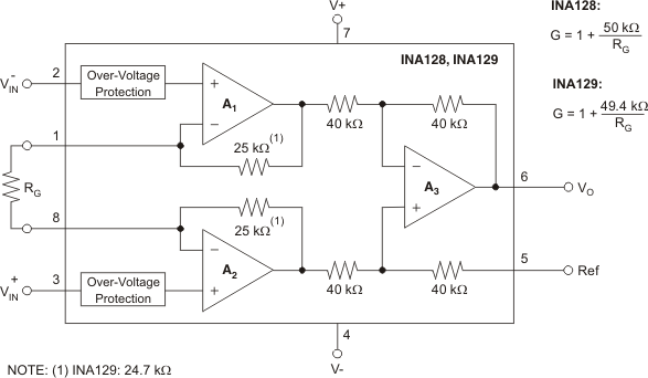
The INA128-HT and INA129-HT are low-power, general-purpose instrumentation amplifiers offering excellent accuracy. The versatile three-operational-amplifier design and small size make them ideal for a wide range of applications. Current-feedback input circuitry provides wide bandwidth even at high gain. A single external resistor sets any gain from 1 to 10000. The INA128-HT provides an industry-standard gain equation; the INA129-HT gain equation is compatible with the AD620.
The INA128-HT and INA129-HT are laser trimmed for very low offset voltage (25 μV Typ) and high common-mode rejection (93 dB at G ≥ 100). These devices operate with power supplies as low as ±2.25 V, and quiescent current of 2 mA, typically. Internal input protection can withstand up to ±40 V without damage.
Texas Instruments' high-temperature products use highly optimized silicon (die) solutions with design and process enhancements to maximize performance over extended temperatures.
The INA129-HT is available in 8-pin ceramic DIP and 8-pin ceramic surface-mount packages, specified for the –55°C to 210°C temperature range. The INA128-HT is available in an 8-pin SOIC-8 surface-mount package, specified for the –55°C to 175°C temperature range.
Device Information(1)
| PART NUMBER | PACKAGE | BODY SIZE (NOM) |
|---|---|---|
| INA128-HT | SOIC (8) | 4.90 mm × 3.91 mm |
| INA129-HT | CFP (8) | 6.90 mm × 5.65 mm |
| CDIP SB (8) | 11.81 mm × 7.49 mm |
- For all available packages, see the orderable addendum at the end of the data sheet.
4 Simplified Schematic
5 Revision History
Changes from E Revision (July 2013) to F Revision
- Added ESD Ratings table, Feature Description section, Device Functional Modes, Application and Implementation section, Power Supply Recommendations section, Layout section, Device and Documentation Support section, and Mechanical, Packaging, and Orderable Information section Go
- Deleted Ordering Information table; for all available packages, see the package option addendum Go
6 Pin Configuration and Functions


Pin Functions
| PIN | I/O | DESCRIPTION | |
|---|---|---|---|
| NAME | NO. | ||
| Ref | 5 | I | Output voltage reference |
| RG | 1, 8 | O | Gain resistor connection |
| V+ | 7 | Power | Positive power supply voltage from 2.25 V to 18 V |
| V– | 4 | Power | Negative power supply voltage from –2.25 V to –18 V |
| V+IN | 3 | I | Non-inverting input voltage |
| V–IN | 2 | I | Inverting input voltage |
| VO | 6 | O | Output voltage |
Bare Die Information
| DIE THICKNESS | BACKSIDE FINISH | BACKSIDE POTENTIAL | BOND PAD METALLIZATION COMPOSITION |
|---|---|---|---|
| 15 mils | Silicon with backgrind | GND | Al-Si-Cu (0.5%) |

Bond Pad Coordinates in Mils
| DESCRIPTION | PAD NUMBER | a | b | c | d |
|---|---|---|---|---|---|
| NC | 1 | –57.4 | –31.1 | –53.3 | –27 |
| V-IN | 2 | –9.85 | –31.4 | –5.75 | –27.3 |
| V+IN | 3 | 25.05 | –31.4 | 29.15 | –27.3 |
| V- | 4 | 56.2 | –34.3 | 60.3 | –30.2 |
| Ref | 5 | 53.75 | –17.6 | 57.85 | –11 |
| VO | 6 | 50.35 | 27.8 | 56.95 | 31.9 |
| V+ | 7 | 7.75 | 30.2 | 11.85 | 34.3 |
| NC | 8 | –57.4 | 28.4 | –53.3 | 32.5 |
| RG(1) | 9 | –57.4 | 13.4 | –53.3 | 20 |
| RG(1) | 10 | –57.5 | 2.7 | –53.4 | 9.3 |
| RG(1) | 11 | –57.5 | –7.9 | –53.4 | –1.3 |
| RG(1) | 12 | –57.4 | –18.6 | –53.3 | –12 |

7 Specifications
7.1 Absolute Maximum Ratings
over operating free-air temperature range (unless otherwise noted) (1)| MIN | MAX | UNIT | |||
|---|---|---|---|---|---|
| Volttage | Supply | ±18 | V | ||
| Analog input | ±40 | ||||
| Current | Output short-circuit (to ground) | Continuous | |||
| Operating temperature | HKJ, HKQ, KGD and JD packages | –55 | 210 | °C | |
| D package | –55 | 175 | |||
| Storage temperature, Tstg | HKJ, HKQ, KGD and JD packages | –55 | 210 | °C | |
| D package | –55 | 175 | |||
7.2 ESD Ratings
| VALUE | UNIT | |||
|---|---|---|---|---|
| A. INA218-HT (D, HKJ, or JDJ Package) | ||||
| V(ESD) | Electrostatic discharge | Human-body model (HBM), per ANSI/ESDA/JEDEC JS-001(1) | ±2000 | V |
| Charged-device model (CDM), per JEDEC specification JESD22-C101(2) | ±50 | |||
| B. INA129-HT (HKQ Package) | ||||
| V(ESD) | Electrostatic discharge | Human-body model (HBM), per ANSI/ESDA/JEDEC JS-001(1) | ±4000 | V |
| Charged-device model (CDM), per JEDEC specification JESD22-C101(2) | ±200 | |||
7.3 Recommended Operating Conditions
over operating free-air temperature range (unless otherwise noted)| MIN | NOM | MAX | UNIT | ||
|---|---|---|---|---|---|
| V power supply | ±2.25 | ±15 | ±18 | V | |
| Input common-mode voltage range for VO = 0 | V - 2 V | V + –2 V | |||
| TA operating temperature INA128-HT | –55 | 175 | °C | ||
| TA operating temperature INA129-HT | –55 | 210 | °C | ||
7.4 Thermal Information: INA128-HT
| THERMAL METRIC(1) | INA128-HT | UNIT | |
|---|---|---|---|
| D [SOIC] | |||
| 8 PINS | |||
| RθJA | Junction-to-ambient thermal resistance | 110 | °C/W |
| RθJC(top) | Junction-to-case (top) thermal resistance | 57 | |
| RθJB | Junction-to-board thermal resistance | 54 | |
| ψJT | Junction-to-top characterization parameter | 11 | |
| ψJB | Junction-to-board characterization parameter | 53 | |
7.5 Electrical Characteristics: INA128-HT
over operating free-air temperature range (unless otherwise noted)| PARAMETER | TEST CONDITIONS |
TA = –55°C to +125°C | TA = 175°C(1) | UNIT | |||||||
|---|---|---|---|---|---|---|---|---|---|---|---|
| MIN | TYP | MAX | MIN | TYP | MAX | ||||||
| INPUT | |||||||||||
| OFFSET VOLTAGE, RTI | |||||||||||
| Initial | TA = 25°C | ±25 ±100/G |
±125 ±1000/G |
µV | |||||||
| vs temperature | TA = TMIN to TMAX | ±0.2 ±5/G |
±1 ±20/G |
±3.5 ±80/G |
µV/°C | ||||||
| vs power supply | VS = ±2.25 V to ±18 V |
±2 ±200/G |
±5 ±500/G |
µV/V | |||||||
| Long-term stability | ±1 ±3/G | ±1 ±3/G | µV/mo | ||||||||
| Impedance, differential | 1010 || 2 | 1010 || 2 | Ω || pF | ||||||||
| Common mode | 1011||9 | 1011||9 | Ω || pF | ||||||||
| Common mode voltage range(2) | VO = 0 V | (V+) − 2 | (V+) − 1.4 | (V+) − 2 | (V+) − 1.4 | V | |||||
| (V−) + 2 | (V−) + 1.7 | (V−) + 2 | (V−) + 1.7 | V | |||||||
| Safe input voltage | ±40 | ±40 | V | ||||||||
| Common-mode rejection | VCM = ±13 V, ΔRS = 1 kΩ |
||||||||||
| G = 1 | 58 | 86 | 58 | 75 | dB | ||||||
| G = 10 | 78 | 106 | 78 | 85 | |||||||
| G = 100 | 99 | 125 | 99 | 110 | |||||||
| G = 1000 | 113 | 130 | 113 | 120 | |||||||
| CURRENT | |||||||||||
| Bias current | ±2 | ±10 | ±45 | nA | |||||||
| vs temperature | ±30 | ±550 | pA/°C | ||||||||
| Offset Current | ±1 | ±10 | ±45 | nA | |||||||
| vs temperature | ±30 | ±550 | pA/°C | ||||||||
| NOISE | |||||||||||
| Noise voltage, RTI | G = 1000, RS = 0 Ω |
||||||||||
| f = 10 Hz | 10 | 10 | nV/√Hz | ||||||||
| f = 100 Hz | 8 | 8 | nV/√Hz | ||||||||
| f = 1 kHz | 8 | 8 | nV/√Hz | ||||||||
| fB = 0.1 Hz to 10 Hz | 0.2 | 0.8 | µVPP | ||||||||
| Noise current | |||||||||||
| f = 10 Hz | 0.9 | pA/√Hz | |||||||||
| f = 1 kHz | 0.3 | pA/√Hz | |||||||||
| fB = 0.1 Hz to 10 Hz | 30 | pAPP | |||||||||
| GAIN | |||||||||||
| Gain equation | 1 + (50 kΩ/RG) |
1 + (50 kΩ/RG) |
V/V | ||||||||
| Range of gain | 1 | 10000 | 1 | 10000 | V/V | ||||||
| Gain error | G = 1 | ±0.01 | ±0.1 | ±0.1% | ±0.5% | ||||||
| G = 10 | ±0.02 | ±0.5 | ±0.5% | ±1% | |||||||
| G = 100 | ±0.05 | ±0.7 | ±0.7% | ±1.5% | |||||||
| G = 1000 | ±0.5 | ±2.5 | ±2% | ±4% | |||||||
| Gain vs temperature(3) | G = 1 | ±1 | ±10 | ±75 | ppm/°C | ||||||
| 50-kΩ resistance(3)(4) | ±25 | ±100 | ±75 | ppm/°C | |||||||
| Nonlinearity | VO = ±13.6 V, G = 1 |
±0.0001 | ±0.001 | ±0.008 | % of FSR | ||||||
| G = 10 | ±0.0003 | ±0.002 | ±0.01 | ||||||||
| G = 100 | ±0.0005 | ±0.002 | ±0.01 | ||||||||
| G = 1000 | ±0.001 | See (5) | ±0.6 | See (5) | |||||||
| OUTPUT | |||||||||||
| Voltage | Positive | RL = 10 kΩ | (V+) − 1.4 | (V+) − 0.9 | (V+) − 1.4 | (V+) − 0.9 | V | ||||
| Negative | RL = 10 kΩ | (V−) + 1.4 | (V−) + 0.8 | (V−) + 1.4 | (V−) + 0.8 | ||||||
| Load capacitance stability | 1000 | 1000 | pF | ||||||||
| Short-circuit current | +6/−15 | +6/−15 | mA | ||||||||
| FREQUENCY RESPONSE | |||||||||||
| Bandwidth, −3 dB | G = 1 | 1300 | 1100 | kHz | |||||||
| G = 10 | 700 | 700 | |||||||||
| G = 100 | 200 | 190 | |||||||||
| G = 1000 | 20 | 17.5 | |||||||||
| Slew rate | VO = ±10 V, G = 10 |
4 | 4 | V/µs | |||||||
| Settling time, 0.01% | G = 1 | 7 | 7 | µs | |||||||
| G = 10 | 7 | 7 | |||||||||
| G = 100 | 9 | 9 | |||||||||
| G = 1000 | 80 | 80 | |||||||||
| Overload recovery | 50% overdrive | 4 | 4 | µs | |||||||
| POWER SUPPLY | |||||||||||
| Voltage range | ±2.25 | ±15 | ±18 | ±2.25 | ±15 | ±18 | V | ||||
| Current, total | VIN = 0 V | ±0.7 | ±1 | ±1 | mA | ||||||
| TEMPERATURE RANGE | |||||||||||
| Specification | −55 | +125 | 175 | °C | |||||||
| Operating | −55 | +125 | 175 | °C | |||||||
7.6 Electrical Characteristics: INA129-HT
over operating free-air temperature range (unless otherwise noted)| PARAMETER | TEST CONDITIONS |
TA = –55°C to +125°C | TA = 210°C(1) | UNIT | |||||||
|---|---|---|---|---|---|---|---|---|---|---|---|
| MIN | TYP | MAX | MIN | TYP | MAX | ||||||
| INPUT | |||||||||||
| OFFSET VOLTAGE, RTI | |||||||||||
| Initial | TA = 25°C | ±25 ±100/G |
±125 ±1000/G |
µV | |||||||
| vs temperature | TA = TMIN to TMAX | ±0.2 ±5/G |
±1 ±20/G |
±1 ±850/G |
µV/°C | ||||||
| vs power supply | VS = ±2.25 V to ±18 V |
±0.2 ±20/G |
±2 ±200/G |
±20 ±1000/G |
µV/V | ||||||
| Long-term stability | ±1 ±3/G | ±1 ±3/G | µV/mo | ||||||||
| Impedance, differential | 1010 || 2 | 1010 || 2 | Ω || pF | ||||||||
| Common mode | 1011||9 | 1011||9 | Ω || pF | ||||||||
| Common mode voltage range(2) | VO = 0 V | (V+) − 2 | (V+) − 1.4 | (V+) − 2 | (V+) − 1.4 | V | |||||
| (V−) + 2 | (V−) + 1.7 | (V−) + 2 | (V−) + 1.7 | V | |||||||
| Safe input voltage | ±40 | ±40 | V | ||||||||
| Common-mode rejection | VCM = ±13 V, ΔRS = 1 kΩ |
||||||||||
| G = 1 | 58 | 86 | 53 | dB | |||||||
| G = 10 | 78 | 106 | 69 | ||||||||
| G = 100 | 99 | 125 | 89 | ||||||||
| G = 1000 | 113 | 130 | 95 | ||||||||
| CURRENT | |||||||||||
| Bias current | ±2 | ±10 | ±50 | nA | |||||||
| vs temperature | ±30 | ±600 | pA/°C | ||||||||
| Offset Current | ±1 | ±10 | ±50 | nA | |||||||
| vs temperature | ±30 | ±600 | pA/°C | ||||||||
| NOISE | |||||||||||
| Noise voltage, RTI | G = 1000, RS = 0 Ω |
||||||||||
| f = 10 Hz | 10 | 25 | nV/√Hz | ||||||||
| f = 100 Hz | 8 | 20 | nV/√Hz | ||||||||
| f = 1 kHz | 8 | 20 | nV/√Hz | ||||||||
| fB = 0.1 Hz to 10 Hz | 0.2 | 2 | µVPP | ||||||||
| Noise current | |||||||||||
| f = 10 Hz | 0.9 | pA/√Hz | |||||||||
| f = 1 kHz | 0.3 | pA/√Hz | |||||||||
| fB = 0.1 Hz to 10 Hz | 30 | pAPP | |||||||||
| GAIN | |||||||||||
| Gain equation | 1 + (49.4 kΩ/RG) |
1 + (49.4 kΩ/RG) |
V/V | ||||||||
| Range of gain | 1 | 10000 | 1 | 10000 | V/V | ||||||
| Gain error | G = 1 | ±0.01% | ±0.1% | ±1.1% | |||||||
| G = 10 | ±0.02% | ±0.5% | ±2.6% | ||||||||
| G = 100 | ±0.05% | ±0.7% | ±13.5% | ||||||||
| G = 1000 | ±0.5% | ±2.5% | ±65.5% | ||||||||
| Gain vs temperature(3) | G = 1 | ±1 | ±10 | ±100 | ppm/°C | ||||||
| 49.4-kΩ resistance(3)(4) | ±25 | ±100 | ±100 | ppm/°C | |||||||
| Nonlinearity | VO = ±13.6 V, G = 1 |
±0.0001 | ±0.001 | ±0.1 | % of FSR | ||||||
| G = 10 | ±0.0003 | ±0.002 | ±0.2 | ||||||||
| G = 100 | ±0.0005 | ±0.002 | ±0.7 | ||||||||
| G = 1000 | ±0.001 | See (5) | ±2.4 | See (5) | |||||||
| OUTPUT | |||||||||||
| Voltage | Positive | RL = 10kΩ | (V+) − 1.4 | (V+) − 0.9 | (V+) − 1.4 | (V+) − 0.9 | V | ||||
| Negative | RL = 10kΩ | (V−) + 1.4 | (V−) + 0.8 | (V−) + 1.4 | (V−) + 0.8 | ||||||
| Load capacitance stability | 1000 | 1000 | pF | ||||||||
| Short-curcuit current | +6/−15 | +12/−5 | mA | ||||||||
| FREQUENCY RESPONSE | |||||||||||
| Bandwidth, −3 dB | G = 1 | 1300 | 850 | kHz | |||||||
| G = 10 | 700 | 400 | |||||||||
| G = 100 | 200 | 50 | |||||||||
| G = 1000 | 20 | 7.5 | |||||||||
| Slew rate | VO = ±10 V, G = 10 |
4 | 4 | V/µs | |||||||
| Settling time, 0.01% | G = 1 | 7 | 10 | µs | |||||||
| G = 10 | 7 | 10 | |||||||||
| G = 100 | 9 | 30 | |||||||||
| G = 1000 | 80 | 150 | |||||||||
| Overload recovery | 50% overdrive | 4 | 4 | µs | |||||||
| POWER SUPPLY | |||||||||||
| Voltage range | ±2.25 | ±15 | ±18 | ±2.25 | ±15 | ±18 | V | ||||
| Current, total | VIN = 0 V | ±0.7 | ±1 | ±2 | mA | ||||||
| TEMPERATURE RANGE | |||||||||||
| Specification | −55 | +125 | 210 | °C | |||||||
| Operating | −55 | +125 | 210 | °C | |||||||

7.7 Typical Characteristics
At TA = 25°C, VS = ±15 V, unless otherwise noted.


| VS = ±15 V | ||


| VS = ±5 V, ±2.5 V | ||


8 Detailed Description
8.1 Overview
The INA12x instrumentation amplifier is a type of differential amplifier that has been outfitted with input protection circuit and input buffer amplifiers, which eliminate the need for input impedance matching and make the amplifier particularly suitable for use in measurement and test equipment. Additional characteristics of the INA12x include a very low DC offset, low drift, low noise, very high open-loop gain, very high common-mode rejection ratio, and very high input impedances. The INA12x is used where great accuracy and stability of the circuit both short and long term are required.
8.2 Functional Block Diagram
8.3 Feature Description
The INA128-HT and INA129-HT are low power, general-purpose instrumentation amplifiers offering excellent accuracy. The versatile three-operational-amplifier design and small size make the amplifiers ideal for a wide range of applications. Current-feedback input circuitry provides wide bandwidth, even at high gain. A single external resistor sets any gain from 1 to 10,000. The INA128-HT and INA129-HT are laser trimmed for very low offset voltage (25 μV typical) and high common-mode rejection (93 dB at G ≥ 100). These devices operate with power supplies as low as ±2.25 V, and quiescent current of 2 mA, typically. The internal input protection can withstand up to ±40 V without damage.
8.4 Device Functional Modes
8.4.1 Noise Performance
The INA128-HT and INA129-HT provide very low noise in most applications. Low-frequency noise is approximately 2 μVPP measured from 0.1 Hz to 10 Hz (G ≥ 100). This provides dramatically improved noise when compared to state-of-the-art, chopper-stabilized amplifiers.

| G ≥ 100 | ||
8.4.2 Input Common-Mode Range
The linear input voltage ranges of the input circuitry of the INA128-HT and INA129-HT are from approximately 1.4 V below the positive supply voltage to 1.7 V above the negative supply. As a differential input voltage causes the output voltage increase, however, the linear input range will be limited by the output voltage swing of amplifiers A1 and A2. So the linear common-mode input range is related to the output voltage of the complete amplifier. This behavior also depends on supply voltage (see Figure 6 and Figure 7).
Input-overload can produce an output voltage that appears normal. For example, if an input overload condition drives both input amplifiers to their positive output swing limit, the difference voltage measured by the output amplifier will be near zero. The output of A3 will be near 0 V even though both inputs are overloaded.